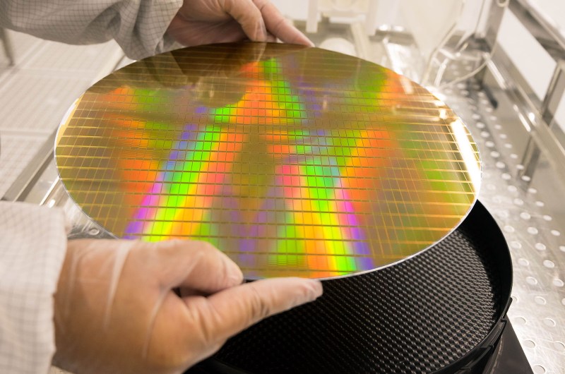
Most of us will probably have seen semiconductor wafers as they trundle their way through a chip factory, and some of us may have wondered about why they are round. This roundness is an obvious problem when one considers that the chip dies themselves are rectangular, meaning that a significant amount of the dies etched into the wafers end up being incomplete and thus as waste, especially with (expensive) large dies. This is not a notion which has escaped the attention of chip manufacturers like TSMC, with this particular manufacturer apparently currently studying a way to make square substrates a reality.
According to the information provided to Nikkei Asia by people with direct knowledge, currently 510 mm x 515 mm substrates are being trialed which would replace the current standard 12″ (300 mm) round wafers. For massive dies such as NVidia’s H200 (814 mm2), this means that approximately three times as many would fit per wafer. As for when this technology will go into production is unknown, but there exists significant incentive in the current market to make it work.
As for why wafers are round, this is because of how these silicon wafers are produced, using the Czochralski method, named after Polish scientist [Jan Czochralski] who invented the method in 1915. This method results in rod-shaped crystals which are then sliced up into the round wafers we all know and love. Going square is thus not inherently impossible, but it will require updating every step of the process and the manufacturing line to work with this different shape.


Why not design hexagonal parts instead and pack them more efficiently into a circle?
I believe it is because they use circular saws that cut in straight lines, so rectangles work better.
Not exclusively. Plasma dicing exists.
Triangles can also work but I have yet to see anyone design with non square/rectangle die. Probably since it’d require a fair amount of change to cut a wafer in 3 different angles rather than 2 and a lot of work for die bonding to frame for IC package. Every other triangle die would have to be rotated 180 or every other frame would need to be rotated 180.
Triangles, square, and rectangle are the only shapes that doesn’t waste any space. All other shapes would require awkward cutting like hexagon, or some wasted silicon spaces like octogon and any odd-numbered polygon higher than 3.
Now I want a penrose tiling of silicon dice
TI could make texagons. https://www.reddit.com/r/Texagon/comments/l8a7lp/perhaps_the_meme_that_started_it_all/
our patio is paved with Cologons, not to be confused with Wyogons :-P
Motorola did make planar triangular transistor die, both BJT and FET back in the late 60’s-early 70’s. I recall pouring glass vials of these onto a glass mirror for wirebonding on my trusty K&S 472. Look in a Motorola 1966 Databook, 2N3904, 2N3906 and JFET’s 2N3821,2N4220. As to IC’s, I don’t recall any of these, but there’s no reason why not if you wanted to.
That was my first thought too
harder to cut after
Cutting and breaking the wafer into hexagonal chips would be a bit difficult.
Apart from the fact that the cutting tools used work in straight lines as stated by Charles Galambos, basically all features on an IC on a silicon substrate follow the crystalline structure of the silicon, which is cubic. Thus square dies can be cut efficiently and cleanly as any chattering is likely to cause crack propagation along the cut line. Cutting on a 45 degree angle to the crystal structure isn’t going to result in good results
Non Manhattan geometry is allowed on some metal layers, and even for the transistor front end layers on processes like hexfet. Plasma dicing also is becoming more common.
‘Cause it’s a PITA in other parts of the design process, would not be worth saving a few (but not all) scraps of silicon around the edges
Processing wafers in any other shape but round is a great challenge. Dry etch will never be able to get the uniformity in the corners within spec. Chambers just dont work like that. This is a non-starter as far as standard RIE process. You would need to make a process chamber with about 800mm process area to make it work. Thats not in the stars any time soon.
Never mind that plasma physics (etch/deposition process) is a lot easier to keep uniform when its round.
450mm were iced somewhere around 2017 as the problems were considered to big and too expensive, so my first reaction to even bigger and “square” is a bit skeptical.
There are good reasons why wafers have been round for 50+ years. From the Czochralski process to wafer lapping to make them flat and other processes.
But I am curious how this will go, even though it has absolutely no practical application for me personally.
But if this is true and it’s more then a “feasibility study”, then I guess Asianometry will make a video about this “soon”. He has by far the best channel about the semiconductor industry as far as I know.
An interesting read of an alternative reason why 450mm wafers have not become widely used:
https://www.theregister.com/2022/08/08/how_tsmc_killed_450mm_wafers/
Also interesting, in the bottom of that article, there is a mention that there is some production of 450mm wafers. But what do you do with them if there are no machines to handle them?
Maybe make square 300mm wafers out of them?
Because this cutting is done early in the production process, it may be cost effective. You still get the higher yield of square wafers, and possibly can put them on currently made wafersteppers.
450mm Si wafers died a good death as being too expensive with only 2-3 possible end users to shoulder the costs of development (450mm consortium at SUNY). These substrates will not be silicon; I would think a glass or polymer which could change the production physics enough to be affordable.
IIRC, growing the raw crystals/ingots requires seed material anyway, so any waste with circular wafers would just be turned around and used as seed for the next crystal/ingot.
I’ve worked on these machines before, their just too fucking big. uniformity is crap for CVD, spin coating works-ish, forget about batch furnace, just too fuggin boingy, litho just cant get the detail out to the edge, 300 mm is king, and likely will be for a long ass time because its so damn convenient
Another nice benefit of round wafers is when a substance is applied and the wafer spun to distribute it. Maybe Si processing has gone past the old days when one would squirt some goo on a wafer and spin it to spread the goo, but that works really well when the wafer is round. If you go for a square-ish wafer, the triangular corners will be subject to different forces than the circular area and goo may not spread as well when the wafer is spun, to say nothing of the spatter coming off the trailing edges of the triangular corners.
The middle bits are subjected to 10x different forces than the outer ring even on circular, so how do they make the middle work at all?
So do they make a ~730mm circle (I’m bad at math sorry), cut off the excess for the 510x515mm and process that?
Don’t quote me on this, but I think they would have to find a new process for making silicon ingots that ended up with a rectangular prism instead of a cylinder. Not sure how difficult/feasible that part is. Otherwise, cutting off parts of the wafer to make it square is just as wasteful as the current problem. If you have a 730mm circular wafer, you’re better off to just use the whole surface area as much as possible. This is why I assume they must be looking for ways to create square wafers from the start of the process instead of cutting circular ones.
More than 25 years ago I read an article in one of the standard EE journals about a process to make square cross-section ingots. It required a square seed and periodically rotating the ingot (or the melt?) 90 degrees during the draw.
As someone working in the semicon lithography industry, color me HIGHLY skeptical on these claims. None of the current high end machines from for instance ASML can handle square wafers, never mind square wafers over 200mm larger than the diameter of the standard 12inch wafer. I’m also not aware of any litho company working on designing a system capable of handling square substrates of that size. The only industry currently using square wafers is solar
yeah im on the wetbench and cvd side of things, lots of retarded problems go away when your round. could you imagine a batch furnace dealing with square wafers!?! uniformity would basically be shit lol
Can’t they fill the spaces on periphery with small ic dies to fill out the wafer?
I’m just a clueless bystander, but my _guess_ would be that; Yes, in principle. But it might be just too fiddly, difficult and costly to separate them.
So even with the prospect of “free” dies, it’s just not worth it ?
Only if those smaller die used the exact same stackup/process as the larger die in the center… this would be an exceedingly rare use case, so practically speaking, ‘no’.
How do you grow a rectangular crystal? Or do you just grow a bigger one and chop off the edge wasting the silicon chunks at the edges? That would wast even more of the waver.
Macro scale crystals follow nanoscale unit cell pattern
Oddball solution.
Nest hexagon and triangle shaped dies so you still only have to cut straight lines.
You lose production volume of the larger H dies, but gain an equal number of smaller T dies.
Another option is simply using triangular dies. You can lay them out so the overall usage of the wafer is a hexagon while maintaining continuous straight cut lines.
At the end of the day there is always going to be waste at the edge.
Is any process change actually going to be worth it for a tiny increase in yields? That work to change the process is itself a loss.
Yeah I can’t see any possible situation in which the peripheral expenses related to this don’t outweigh whatever savings you’d get in a reasonable timeframe
Seems like this would be more useful for the solar cell industry, IMO. I can’t imagine the tiny amount of waste from clipping off the edge of a circle is a significant factor in the cost of most chips.
i think there is a big misunderstanding!
TSMC is planing to go to 510×515 substrates, read this carefully, substrates! Thats the part where they place things onto it.
Where do they write that the source, the thing where the parts are from will switch out from 12″(300mm) round discs?
As i read it, currently both the source and the substrate are 300mm discs, but they want to switch the substrate into a 510×515 plane. And this substrates are not SI, that might get glass core someday but now its a PCB.
Maybe getting ready for power delivery on the backside.
Spot on, Steff. I think Maya read this one incorrectly. What TSMC is talking about is a multi-material approach, NOT replacing 12″ (round) wafers altogether with bigger (square) wafers.
This article (not behind a sign-up paywall like the original linked article, BTW) gives a better overview:
https://www.tweaktown.com/news/98944/tsmc-exploring-radically-new-semiconductor-packaging-technique-called-panel-level/index.html
Right – so to use old skool terminology, hybrid circuits are getting bigger.
With more chiplets on them.
Wasting sand vs replacing the entire facility, that’s an easy call.
“He Czochralski) made this discovery by accident: instead of dipping his pen into his inkwell, he dipped it in molten tin, and drew a tin filament, which later proved to be a single crystal.”
Cool example of serendipity. But who has pots of molten tin on their desk? Or maybe: why?
So the concept is to slice up a boule like lumber rather than salami?
I don’t know about reflective optics, but lenses tend to produce imaging circles.
Czochralski method:
“He made this discovery by accident: instead of dipping his pen into his inkwell, he dipped it in molten tin, and drew a tin filament, which later proved to be a single crystal”
WTF
Incidentaly, since there is no mention of how those squares come about I’d guess they just cut off the edges of a round rod in advance then eh? Before slicing it into wafers you think? Or after slicing but before it goes into the machines.
Anyway, as the article states: “commercialization could take several years.”