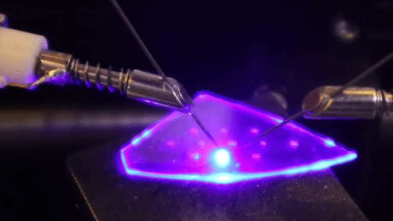
An irregular shard of a crystal wafer is set on a table, with two wire probes contacting it. Between the probes, a bright blue-purple light glows, illuminating the rest of the wafer.

Making LEDs In The Home Fab

Impressive as it most certainly is when an amateur fabricates a semiconductor, most of the projects we’ve seen are more demonstrations than workable chips. [Dr. Semiconductor], however, is going much further with his fabrication process, and is already working on a method to bond chips to printed circuit boards. It’s difficult to align a PCB with the pads on the underside of an opaque silicon wafer, however, so as a trial run he’s made and bonded some transparent LED chips.

The starting material for these chips is a gallium nitride (GaN) LED epiwafer, a stacked structure of n-doped GaN, an indium gallium nitride quantum well layer, and p-doped GaN grown on a sapphire substrate. When current passes through the structure, electrons from the n-doped layer and holes from the p-type layer recombine in the quantum well layer, emitting blue light. To make a functional LED from this, [Dr. Semiconductor] needed to make electrical contacts to both the n-type and p-type layers. Making the n-type contact required cutting through the p-type and quantum well layers.

This would normally be done with reactive ion etching in chlorine, but [Dr. Semiconductor] came up with a new process: a 355-nm ultraviolet etching laser causes GaN to break down into gallium and nitrogen, with the resulting cut being cleaned up by a potassium hydroxide etch. To deposit the contacts themselves, [Dr. Semiconductor] formed a photoresist mask, deposited metal (nickel, silver, and titanium) in a sputtering chamber, and used a developer solution to dissolve the mask and lift off the unwanted metal regions.
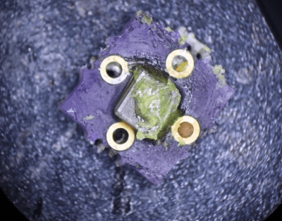
A square, purple PCB is shown under a microscope. The PCB has four vias surrounding a transparent chip, which has a blob of translucent yellow material on top of it.
The LED after bonding and phosphor application.

When [Dr. Semiconductor] applied current between the two contacts, the LED glowed bright blue. The next step was to mount it to a PCB; to do so, he first sliced the wafer into individual LED chips with the ultraviolet laser. He then electroplated indium bumps onto a printed circuit board, positioned the chip above these bumps, added some rosin flux, and melted the indium bumps. This soldered the chip to the board and let the board power the LED.

Like most commercial white LEDs, these were blue; most LED assemblies additionally include a phosphor layer which absorbs blue light and emits another color. To create a white LED, for example, [Dr. Semiconductor] mixed cerium-doped yttrium aluminium garnet phosphor powder with clear silicone and spread it over the LED. This absorbs some of the blue light and emits yellow light, and the resulting mixture of blue and yellow light looks white to human eyes.

We’ve previously covered some of the history of LEDs and the phosphors which make them useful. This seems to be the first inorganic LED we’ve seen, but we’ve also seen a few homemade OLEDs.

Thanks to [SpuriousIndices] for the tip!
Creating 1 Um Features The Hacker Way

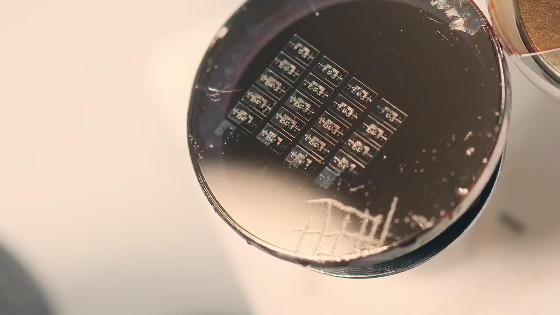
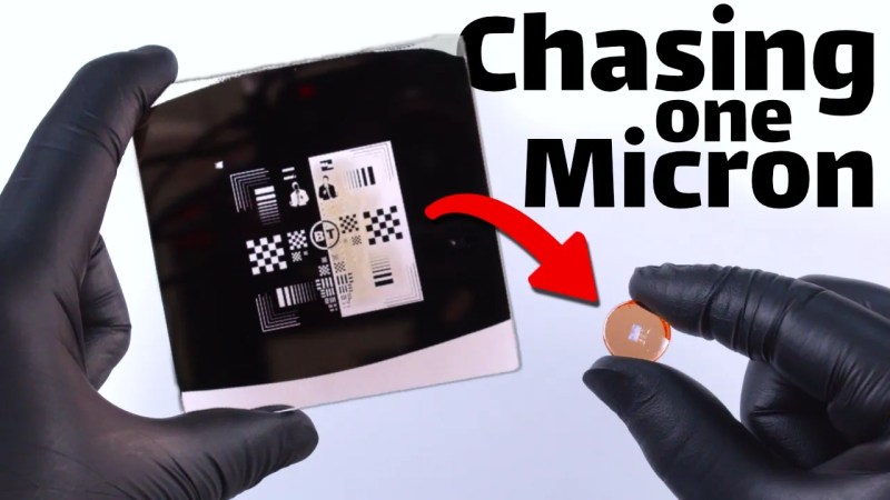
[Breaking Taps] has done some lithography experiments in the past, including some test patterns and a rudimentary camera sensor. But now, it’s time to turn it up a notch with 1µm garage semiconductor ambitions.

The e-beam lithography he’s done in the past can achieve some impressive resolutions, but they aren’t very fast; a single beam of electrons needs to scan over the entire exposure area, somewhat like a tiny crayon. That’s not very scalable; he needed a better solution to make 1µm semiconductors.

Test patterns from the first attempt

In his quest, he starts by trying to do maskless photolithography, using a literal projector to shine light on the target area all at once. After hacking a projector devkit apart, replacing blue with ultraviolet and adding custom optics, it’s time for a test. The process works for the most part but can’t produce fine details the way [Breaking Taps] needs. Unfortunately, fixing that would mean tearing the whole set-up apart for the umpteenth time.
Continue reading “Creating 1 Um Features The Hacker Way”

TSMC’s Long Path From Round To Square Silicon Wafers

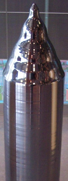
Crystal of Czochralski-grown silicon.

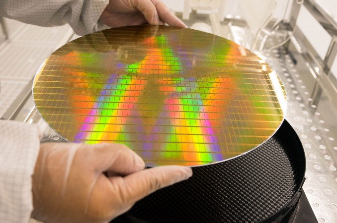
Most of us will probably have seen semiconductor wafers as they trundle their way through a chip factory, and some of us may have wondered about why they are round. This roundness is an obvious problem when one considers that the chip dies themselves are rectangular, meaning that a significant amount of the dies etched into the wafers end up being incomplete and thus as waste, especially with (expensive) large dies. This is not a notion which has escaped the attention of chip manufacturers like TSMC, with this particular manufacturer apparently currently studying a way to make square substrates a reality.

According to the information provided to Nikkei Asia by people with direct knowledge, currently 510 mm x 515 mm substrates are being trialed which would replace the current standard 12″ (300 mm) round wafers. For massive dies such as NVidia’s H200 (814 mm2), this means that approximately three times as many would fit per wafer. As for when this technology will go into production is unknown, but there exists significant incentive in the current market to make it work.

As for why wafers are round, this is because of how these silicon wafers are produced, using the Czochralski method, named after Polish scientist [Jan Czochralski] who invented the method in 1915. This method results in rod-shaped crystals which are then sliced up into the round wafers we all know and love. Going square is thus not inherently impossible, but it will require updating every step of the process and the manufacturing line to work with this different shape.

Hackaday Links Column Banner

Hackaday Links: May 12, 2024

Don’t pack your bags for the trip to exoplanet K2-18b quite yet — it turns out that the James Webb Space Telescope may not have detected signs of life there after all. Last year, astronomers reported the possible presence of dimethyl sulfide there, a gas that (at least on Earth) is generally associated with phytoplankton in the ocean. Webb used its infrared spectrometer instruments to look at the light from the planet’s star, a red dwarf about 111 light-years away, as it passed through the hydrogen-rich atmosphere. The finding was sort of incidental to the discovery of much stronger signals for methane and carbon dioxide, but it turns out that the DMS signal might have just been overlap from the methane signal. It’s too bad, because K2-18b seems to be somewhat Earth-like, if you can get over the lack of oxygen and the average temperature just below freezing. So, maybe not a great place to visit, but it would be nice to see if life, uh, found a way anywhere else in the universe.

Attention Fortran fans: your favorite language isn’t quite dead yet. In fact, it cracked the top ten on one recent survey, perhaps on the strength of its numerical and scientific applications. The “Programming Community Index” is perhaps a bit subjective, since it’s based on things like Google searches for references to particular languages. It’s no surprise then that Python tops such a list, but it’s still interesting that there’s enough interest in a 67-year-old programming language to make it onto the list. We’d probably not advise building a career around Fortran, but you never know.

Continue reading “Hackaday Links: May 12, 2024”