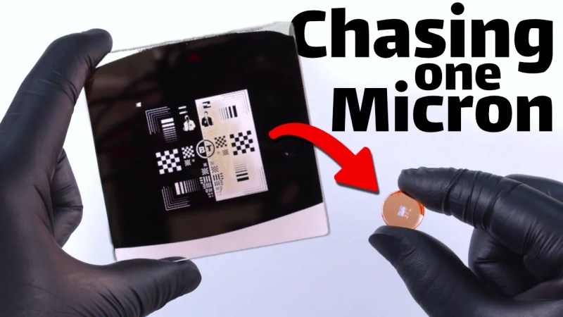
[Breaking Taps] has done some lithography experiments in the past, including some test patterns and a rudimentary camera sensor. But now, it’s time to turn it up a notch with 1µm garage semiconductor ambitions.
The e-beam lithography he’s done in the past can achieve some impressive resolutions, but they aren’t very fast; a single beam of electrons needs to scan over the entire exposure area, somewhat like a tiny crayon. That’s not very scalable; he needed a better solution to make 1µm semiconductors.
In his quest, he starts by trying to do maskless photolithography, using a literal projector to shine light on the target area all at once. After hacking a projector devkit apart, replacing blue with ultraviolet and adding custom optics, it’s time for a test. The process works for the most part but can’t produce fine details the way [Breaking Taps] needs. Unfortunately, fixing that would mean tearing the whole set-up apart for the umpteenth time.
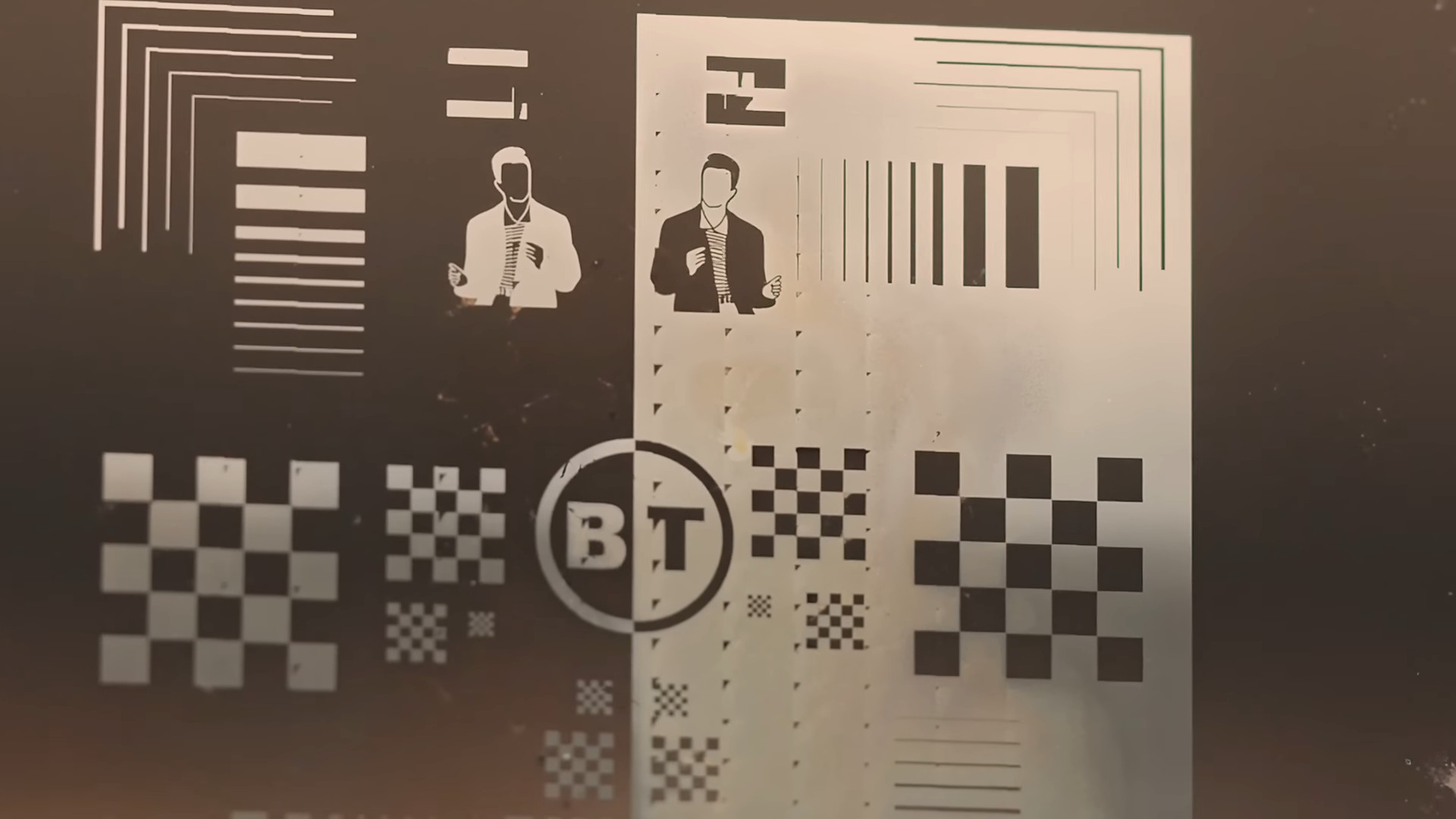
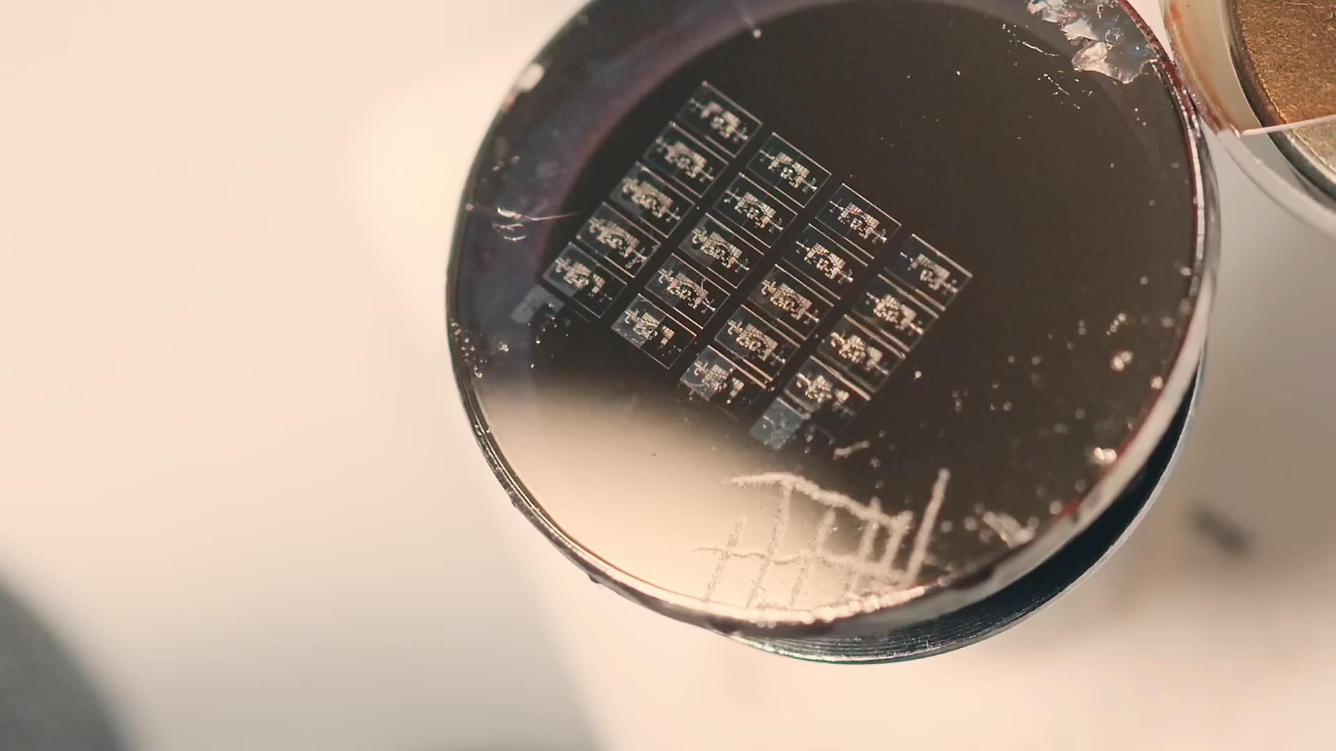
In either a genius move, or the typical hacker tangent energy, he decides not to completely re-build the maskless lithography machine, but instead uses it to create masks for use in a 10:1 reduction machine, also known as the more traditional mask photolithography. In the end, this works out well for him, reaching just about 2 µm effective minimum feature size in this two-step process.
We haven’t even remotely covered everything and there are, of course, always things to improve. And who knows? Maybe we’ll see 1µm semiconductors from [Breaking Taps] in the future.


The engineering and design effort he puts in to solve his problems, and the thought that goes into debugging the new problems that arise, always impress me about his work.
“1µm garage semiconductor ambitions”
Some garages are more equal than others.
My most challenging ambition for my garage is to maintain enough open space to park a car.
Don’t talk crazy, man. It’s a pipe dream and you know it.
Ha! I gave up on that ages ago and so my garage is full of tools and workbenches (welding, rudimentary machining, chem lab with fume hood, and a nice docking area with twin 32″ 4k monitors) and the car just has to lump it and stay in the driveway.
“My most challenging ambition for my garage is to maintain enough open space to park a car.” Sounds very familiar for some reason :) .
Neat project. Talk about dedication!
Does anyone know what camera he is using for his litho system?
Having been a mask making engineer in the 1 micron era, it’s fun to see a modern hacking approach to the tools needed to print 1 micron features. Only observation is it would be unusual for a lens to focus red and UV light the same. In some cases, it may work by accident https://en.wikipedia.org/wiki/Apochromat
The DMD with some optics could make for the perfect portable device to do some photolithography on photoresist covered copper clad boards. Just put the device on a copper clad board, and in a few minutes the photoresist will be ready for etching.
I’d definitely buy if something like that commercially existed.
The annoying thing is that TI does make DMDs optimized specifically for the 400nm-region for SLA 3D printers, but they don’t have any demo boards like they do for the normal DMDs.