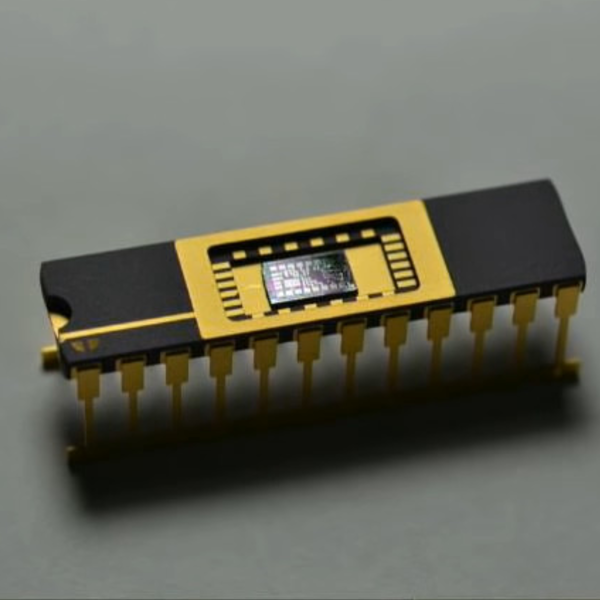
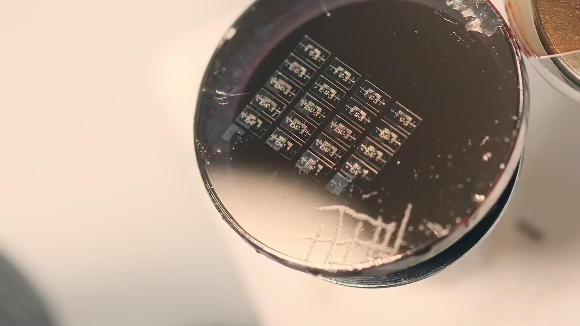
[Breaking Taps] has done some lithography experiments in the past, including some test patterns and a rudimentary camera sensor. But now, it’s time to turn it up a notch with 1µm garage semiconductor ambitions.
The e-beam lithography he’s done in the past can achieve some impressive resolutions, but they aren’t very fast; a single beam of electrons needs to scan over the entire exposure area, somewhat like a tiny crayon. That’s not very scalable; he needed a better solution to make 1µm semiconductors.
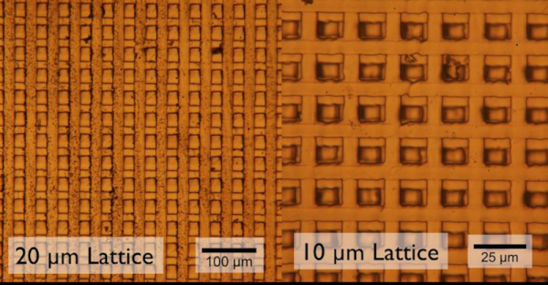
In his quest, he starts by trying to do maskless photolithography, using a literal projector to shine light on the target area all at once. After hacking a projector devkit apart, replacing blue with ultraviolet and adding custom optics, it’s time for a test. The process works for the most part but can’t produce fine details the way [Breaking Taps] needs. Unfortunately, fixing that would mean tearing the whole set-up apart for the umpteenth time.
Continue reading “Creating 1 Um Features The Hacker Way”