[Hans Rosenberg] knows a thing or two about RF PCB design and has provided a three-part four-part video demonstration of some solid rules of thumb. We will cover the first part here and leave the other two for the more interested readers!
The design process begins with a schematic diagram, assuming ideal conductors. Advanced software tools can extract the resistive, inductive, and capacitive elements of the physical wiring to create a parasitic model that can be compared to the desired schematic. The RF designer’s task is to optimize the layout to minimize differences and achieve the best performance to meet the design goals. However, what do you do when you don’t have access to such software?
[Hans] explains that at low frequencies, return current flows through all paths, with the lowest resistance path taking most of the current. At higher frequencies, the lowest inductance path carries all the current. In real designs, a ground plane is used instead of an explicit return trace for the lowest possible impedance.
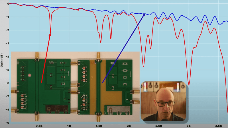
[Hans] shows the effect of interrupting the signal return path on a physical test PCB. The result is pretty bad, with the current forced to detour around the hole in the ground plane. A nanoVNA shows a -20 dB drop at 4 GHz, where the ground plane has effectively become an antenna. Energy will be radiated out, causing signal loss, but worse, it will create an EMC hazard with an unintended transmission.
Additionally, this creates an EMC susceptibility, making the situation worse. Placing a solder blob to bridge the gap directly under the signal trace is all that’s required to make it a continuous straight path again, and the performance is restored.
Floating planes are also an issue in RF designs, causing signal resonance and losses. One solution is to pull back the planes near the signal or stitch them to the ground plane with vias placed closely on either side of the signal trace. However, such stitching may slightly affect transmission line impedance and require tweaking the design a little. The next two parts of the series expand on this, hammering home the importance of good ground plane design. These are definitely worth a watch!
PCB design is as much art as science, and we’ve discussed this subject a lot. Here’s our simple guide to rocking RF PCB designs. There’s also a lot of devil in that detail, for example when understanding edge-launch SMA connectors.
( Updated to add part 4. Thanks [MacGyverS2000] !)


In the last video would a “via shield” help? So many vias under the shield component to the ground plane at the bottom layer. And what about making a thin slot in the PCB and have the shield go through the PCB ?
The reason for the poor isolation is when you’re working with the 2L design, you’re compensating for the large inductance (trace/ground spacing) by adding a large capacitance (trace width) – the impedance is the ratio of inductance to capacitance. But that doesn’t change the fact that the field’s just… stronger, period. Think about it – you’re storing more charge, so if you just probed the electric/magnetic fields there, they’d be bigger – and then waving your hand above it obviously is going to change it. It actually helps with resistive losses (I mean… it’s a bigger trace, so duh) but those don’t matter.
Now think about an actual metal shield – yes, it’ll block other things from interacting, but now you’ve got a giant metal object and you’ve still got big inductance/capacitance. You can even just think about it in a physical sense: imagine the field puffing out from the board, and you “squish” it with a shield – you’re going to get more coupling across your components, and the filter’s going to do worse.
You really just want a low inductance and low capacitance, which means you want to bring the ground closer. So just… do it.
Remember he said that the top/gnd spacing was 0.19 mm in the 4 layer design? That’s 7.5 mils. The crappiest PCB manufacturer on the planet nowadays can do 7.5 mil spacing! So just… bring the ground closer to the trace, and make the trace narrower.
That’s what a coplanar waveguide (CPW) structure is. When it’s got a ground plane some distance away, it’s CPW-G (coplanar waveguide with ground).
The problem is that there are no exact analytical formulas for CPW-G (like there are for microstrip), and a lot of the calculators on the Web are, well, wrong. I actually use a program called atlc (Arbitrary Transmission Line Calculator) to tweak CPWG impedances in designs. It’s a little clunky, but I’ve found it’s a heckuva lot lighter weight than something like openEMS.
With a CPW-G structure you can bring the ground extremely close (most PCB houses are 4-5 mils trace/space at this point). The only real downside to CPW structures is that at very high frequencies with cheap substrate they’ll be a bit lossier because more of the field is in the dielectric than free space: but on the plus side, they’re also less dispersive since the field’s in a more uniform dielectric.
Interesting comment, huge thank you for the ATLC recommendation as I didn’t know about it, but I have some questions.
I don’t get your remark on losses being worse in a CPW. I thought it was the other way around: in a microstrip, almost all of the field is in the dielectric so CPW has less loss because at least some of the field was in air. And for the more uniform dielectric medium, isn’t it better in a microstrip?
Also, cheap PCB manufacturers now offer inexpensive 4 layer stackups, with a dielectric thickness of 3 or 4 mils (see JLCPCB). So I guess you can bring the ground as close as with a 4 mil spaced CPW? With the benefit of not having to think about closely via stitching the ground pour and worry about the effect of the via’s on the line impedance, having presumably less effects of using soldermask or ENIG plating on the copper, etc.
CPW conductor losses are higher, because the geometry is smaller (if you moved the plane closer so the microstrip width is equal, the differences would be small).
For repeatability, I meant it’s more repeatable manufacturer to manufacturer (it’s easier to transfer between fans) since the geometry is copper defined. Microstrip is more repeatable batch to batch, but again those are very high frequency effects.
Fabs, not fans. Stupid autocorrect.
There’s a lot of competing effects that change things as frequencies increase, but if you really want to eke out performance you should be thinking CPW-G all the time: it’s just a case of how coupled you want it to be to the top or bottom. Even the example here is actually CPW-G, it’s just so loosely coupled at the top layer it’s microstrip-like.
The problem with thinking pure microstrip is there are no knobs to turn. The layer height is what it is.
There’s a Part 4, added just a couple of weeks ago:
https://www.youtube.com/watch?v=vumYrebIXm0
Only going through part 1, the reason why you put a ground plane on either side of the trace is to make a coplanar waveguide structure: leaving the trace thickness as microstrip is what kills you.
The benefit of coplanar waveguide is that PCB manufacturing’s gotten accurate enough that you can make a reasonably-sized CPWG structure by making the ground pour spacing small: and in fact, it typically hits impedance targets more repeatably than microstrip because the copper distances are far more repeatable than the PCB thicknesses and dielectric constants, although you might need to tweak a design once or twice.
The other benefit of CPWG is that it’s got better isolation and it’s less dependent on enclosures: with microstrip, if you put a circuit in a shielded box, it’ll change its characteristics a lot, because microstrip assumed free air above it and a lot of the signal was propagating there. With CPWG – especially tightly-coupled CPWG – the field is tightly constrained close to the board.
Those edge-mount connectors are intended for a CPWG structure – in some of the more expensive connectors the example design is very explicitly CPWG.
The article illustration made me think about this Eric Bogatin interview, where he talks (around the end) about some simulation and measurements on the bad effect of copper pour near PCB traces.
https://www.youtube.com/watch?v=h9yyOmL8duE
Hi, this is the actual ‘Hans Rosenberg’. I’m completely surprised my videos ended up here on this platform. I saw a big spike in my views and traced it here. Very honored you’re posting my material here. I’m going to keep making content like this when I get back from vacation. I’ll be covering audio design, RF design, high performance transistor amplifier design, antenne design. Will take some time to make all these videos, each one takes around 4 days of full time work, but I have a year :-)
Best regards,
Hans Rosenberg