When we think of assembling a PCB, we’re almost always thinking about solder. Whether in paste form or on the spool, hand-iron or reflow, some molten metal is usually in the cards. [Stephen Hawes] is looking for a solderless alternative for prototyping, and he shows us the progress he’s made toward going solderless in this video.
His ulterior motive? He’s the designer of the LumenPNP open-source pick-and-place machine, and is toying with the idea of a full assembly based just on this one machine. If you strapped a conductive-glue extruder head on the machine in addition to the parts placer, you’d have a full assembly in one step. But we’re getting ahead of ourselves.
[Stephen] first tries Z-tape, which is really cool stuff. Small deformable metal balls are embedded in a gel-like tape, and conduct in only the Z direction when parts are pushed down hard into the tape. But Z-tape is very expensive, requires a bit of force to work reliably, and [Stephen] finds that the circuits are intermittent. In short, Z-tape is not a good fit for the PNP machine.
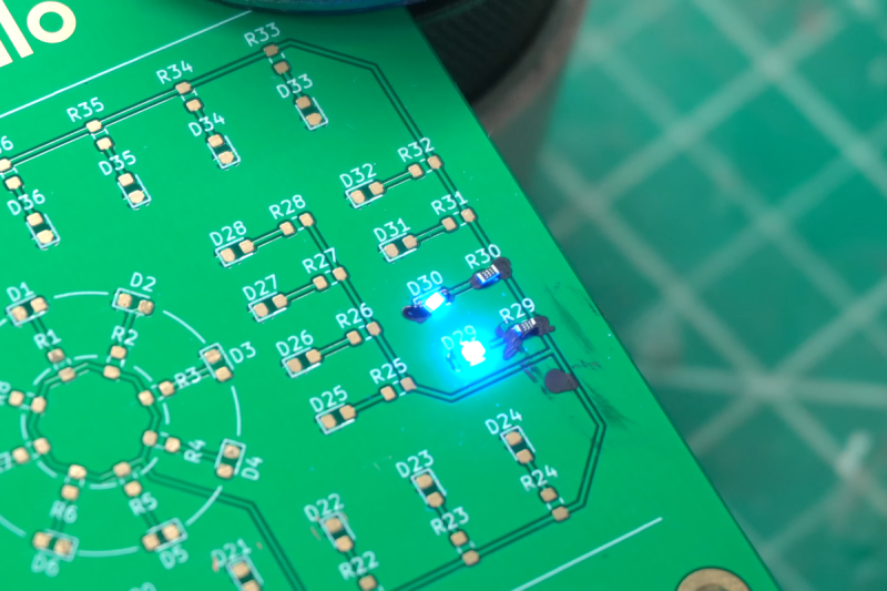
But what [Stephen] does find works well is a graphite-based conductive glue. In particular, he likes the Bare Conductive paint. He tries another carbon-based paint, but it’s so runny that application is difficult, while the Bare stuff is thick and sticky. (They won’t tell you their secret formula, but it’s no secret how the stuff is basically made.) That ends up looking very promising, but it’s still pretty spendy, and [Stephen] is looking to make his own conductive paste/paint pretty soon. That’s particularly appealing, because he can control the stickiness and viscosity, and he’ll surely let us in on the secret sauce.
(We’re armchair quarterbacking here, but the addition of a small amount of methyl cellulose and xanthan gum works to turn metal powder into a formable, printable metal clay, so it might make a carbon paste similarly adjustably sticky.)
We love the end-goal here: one machine that can apply a conductive paint and then put the parts into the right place, resulting in a rough-and-ready, but completely hands-off assembly. You probably wouldn’t want to use this technique if the joint resistance was critical, or if you needed the PCB to stand up to abuse. There’s a reason that everyone in industry uses molten metal, after all. But for verifying a quick one-off, or in a rapid-prototyping environment? This would be a dream.
We’ve seen other wacky ways to go solderless before. This one uses laser-cut parts to hold the components on the PCB, for instance. And for simply joining a couple wires together, we have many more solutions, many thanks to you all in the comments!


Seems like a fun project, it would be pretty cool if a PnP machine could replace the reflow process. Although I’m not sure it will save much time at all.
Back when I was a child, I made my own version of a conductive paste by adding salt to dough slurry. It was a fun experiment, lighting LEDs with thin strips of watery dough.
That just takes the biscuit.
In Aerospace aluminum is expoxied to aluminum and frequently needs to be conductive. I believe the epoxy is filled with aluminum or silver to create the final conductive bond.
So, I was wondering, since there are laser based soldering techniques, why not apply solder paste with a stencil, place components using the pick and place machine, and then use a laser mounted on the head and appropriate software to individually solder all the points?
It will be slow (probably), but it will be automatic. Apply solder paste and set the board onto the machine and come back in a few hours or the next morning to a assembled and soldered PCB.
+1 ….. that was my immediate thought (about 30 seconds in)
AFAIK this actually exists but its quite expensive and doesn’t really offer any advantages over reflow, plus it cannot do QFN or BGA since the pads are not exposed
This. Part limitations, cost, and for all but the simplest, no real gain in time. Reflow is well understood.
When I was a student there was a project running to do precisely that. There was a stack of bricks against the back wall, behind where the PCB would be. There were several small holes with glassy dribbles on many of the bricks. Obviously they forgot to occasionally turn the power down from “Vapourise Planet”.
As others have said laser soldering has been around for a while, just like making PCBs by burning the copper off.
They usually use high-power UV lasers, so a bit out of reach for most people.
Laser soldering falls under the “selective soldering” category, where you do a second run to add “special” parts or where you don’t want to run the board thru reflow again for whatever reason. Temperature sensitive, hard to pick & place, connectors on the back of your board and so on. Usually easier to design around those problems.
Because he didn’t want to
Honestly this guy always seems like he’s just railed a ton of coke and then hit “record” before making the most insanely over-enthusiastic videos about surface mounting components. There’s people out there bungee-jumping with less excitement than this guy talks about SMT.
He seems to have suffered mission creep and multiple wheel reinventions along the way, last update I saw about his PnP they were trying to re-invent the flow solder machine using cheap solder baths and wishful thinking rather than just buy or rent the right tool for the job that already exists. I kinda wonder if this solderless thing is the same, these days soldering is neither difficult nor expensive so I’m not sure what the benefit is.
Agree. If the PnP can dispense solder paste, it can so it on a Infrared heated’s plate. Then using a heat gun to solder is a simple process. Or simply moving the panel with components and solder paste to the oven isn’t a big deal anyway in the whole process.
Stephen is quite enthusiastic in his videos, yes. I’ve seen that a lot among YouTubers and I think it’s a style thing.
Largely his channel these days is about Opulo the company, and how they’re approaching problems. When it comes to PCB assembly in particular, I think they try really hard to avoid buying ‘The right machine for the job’, because their business is finding solutions for much smaller scale operations. The right machine for through-hole production soldering is a wave-flow machine on a conveyor. One of the amusing followups to that video was when they revv’d the motherboard and said “Wait, we make a PnP – why are we even using through-hole parts?”
All of that said, I think this is more of a “wouldn’t that be cool?” concept, rather than pursuing an actual production technique. Of course, that’s how you discover new things…
Oh wait, this is literally just replacing the act of soldering? Yeah, I don’t get who would be asking for that.
I assumed it was about a machine to create and populate a PCB in one step, which certainly would be useful.
We can put man on the Moon but not figure this out?
I like this video, I love the enthusiasm that Stephen displays here, I especially like that he’s identified and talked about solder paste and ovens being the right way to do solid connections especially as that wasn’t his primary goal, his primary goal seems to be ‘can I do all of this purely with the mechanics of a pick and place machine. Sometimes these side missions are the best part of the journey, can’t wait to see where this path leads.
Interesting project. I wish him well.
When I was an undergrad (‘late 89s /early 90s) we used wire wrapping extensively for all our project prototyping. I never understood why it seems to have fallen out of favor or maybe it was niche.
It was easy to use and more importantly easy to correct. It was also very robust .I know it was also used quite a bit in aerospace industry too. Attempted to find some online many years ago, but very few seemed to have even heard of it.