
Usually when we present a project on these pages, it’s pretty cut and dried — here’s what was done, these are the technologies used, this was the result. But sometimes we run across projects that raise far more questions than they answer, such as with this printed circuit board that’s actually printed rather than made using any of the traditional methods.
Right up front we’ll admit that this video from [Bad Obsession Motorsport] is long, and what’s more, it’s part of a lengthy series of videos that document the restoration of an Austin Mini GT-Four. We haven’t watched the entire video much less any of the others in the series, so jumping into this in the middle bears some risk. We gather that the instrument cluster in the car is in need of a tune-up, prompting our users to build a PCB to hold all the instruments and indicators. Normally that’s pretty standard stuff, but jumping to the 14:00 minute mark on the video, you’ll see that these blokes took the long way around.
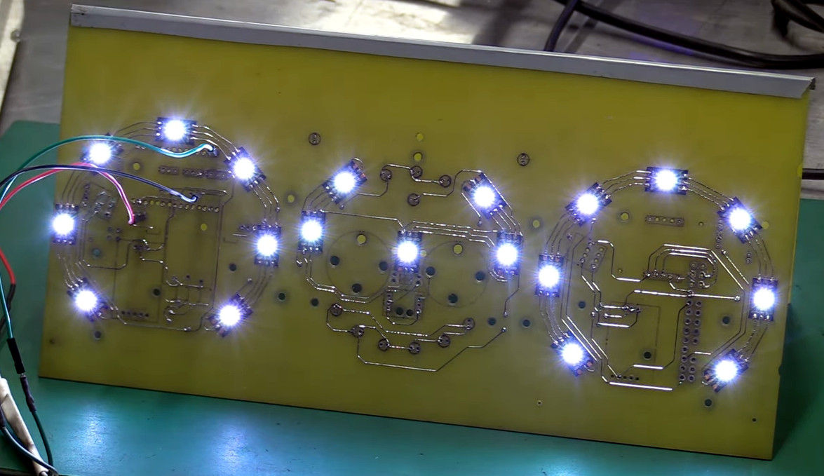 Starting with a naked sheet of FR4 substrate, they drilled out all the holes needed for their PCB layout. Most of these holes were filled with rivets of various sizes, some to accept through-hole leads, others to act as vias to the other side of the board. Fine traces of solder were then applied to the FR4 using a modified CNC mill with the hot-end and extruder of a 3D printer added to the quill. Components were soldered to the board in more or less the typical fashion.
It looks like a brilliant piece of work, but it leaves us with a few questions. We wonder about the mechanics of this; how is the solder adhering to the FR4 well enough to be stable? Especially in a high-vibration environment like a car, it seems like the traces would peel right off the board. Indeed, at one point (27:40) they easily peel the traces back to solder in some SMD LEDs.
Also, how do you solder to solder? They seem to be using a low-temp solder and a higher temperature solder, and getting right in between the melting points. We’re used to seeing solder wet into the copper traces and flow until the joint is complete, but in our experience, without the capillary action of the copper, the surface tension of the molten solder would just form a big blob. They do mention a special “no-flux 96S solder” at 24:20; could that be the secret?
We love the idea of additive PCB manufacturing, and the process is very satisfying to watch. But we’re begging for more detail. Let us know what you think, and if you know anything more about this process, in the comments below.
Thanks to [dennis1a4] and about half a dozen other readers for the nearly simultaneous tips.


They mention the use of spray on adhesive later in the video when pointing out the dirt that got stuck to it. I assume they sprayed the adhesive on the FR4 before printing the traces on. And they tested a trace to destruction, reaching 5 amperes.
The original traces were just deposited directly on the board (when molten, it conforms to the rough surface which is enough to provide some mechanical adhesion.) It’s only when they printed traces separately and then transferred them to the board that they needed to add additional adhesive.
Neither is sufficient for an automotive application! But they’ve done all the design work, transferring this to gerbers and getting a commercial PCB made would be trivial now.
It´s low likely low-temperature solder. While it can pass some current, it is very brittle. It might work at the beginning, but it likely won´t hold very long.
I would have just buy a big sheet of FR4 or even a bakelite plate with one copper side (affordable), drill all the holes in the right place, then just draw the tracks with a pen before etching, like in the old days of yore. If you ask a PCB fab for such a big piece, it would be very expensive.
You can use 3d printer to draw traces. Heck, there is a hack to use laser printer
A hack to use a laser printer? I’ve been doing it that way since ’93…
Are there other methods that folks are using these days?
I am not aware of any spray-on adhesive that will adhere solder to a board with even a tiny fraction of the bond of a typical copper-to-FR4 bond, but interesting nonetheless – maybe some potential for fast prototyping but certainly not appropriate for production due to the mechanical properties of solder. Maybe they could try extruding conductive epoxy for something a little bit more robust.
Voltera has a machine that, among other things, deposits some kind of solder like this. Never got to try it – our supply dried out before we could get the software installed and they wanted to charge for every refill.
It’s made clear in the video that it is a prototype.
In rugged electronics certain coat is used that covers pcb and elements.
But whoever presented this wrong about one thing: the novelty of method. It’s goddamn the OLDEST method to do this, which was quickly discarded because flux and I perfections would eventually destroy lines traced by solder. It’s what we were running away from for long time – usage of large volumes of flux by using smd and alike – less solder volume means less possible “poisoning”, cracking, other defects in soldering which would lead to failure
It’s a prototyping setup.
One that allows rapid and repeated iterations of the design.
It’s not meant to stand up to normal use.
High temp, no flux solder for the traces, low temp to attach components.
Spray glue was use when replacement tracks were printed separately and then placed on the board. Needed because an electrical fault was interrupting prints.
All the information is in the video.
when your hammer is a well equipped machine shop…
Definitely an admirable effort with good looking results, with a retro / steampunk vibe as bonus. I applaud it as a hack, but the time and effort seems misspent when considering the actual project on hand.
Yep. Yep. That’s project Binky. This is, what, about year seven of a two-year project?
The first video was uploaded 11 years ago. So probably closer to 12 years by now
And this episode of weapons-grade yak shaving has been at least 2 years in the making for what could easily have been a couple of $50 JLC orders.
Agreed, much effort and time for this solution but nice hack.
But tracks could fall off and create shorts over time/temperature/vibration, especially in a car and you still need to place the rivets/PTH by hand and those are not cheap.
If there was a one stop solution for quick prototype as we do have for 3DP, that would be great, in the meantime, I’m still ordering online and get a perfect PCB in a week, we are so lucky to have such online services.
“One that allows rapid and repeated iterations of the design.”
And it’s quite cheap as well. If you have a new iteration of the prototype, you just scrape the traces off the board and have a clean piece of FR4. The solder that you scraped off goes back into the feeder of the extruder. Leaves the problem of the holes and VIAs, but you can tweak your iteration to reuse them as much as possible. So all in all, it seems to me that it’s quite economic. There is a lot of reuse and recycling in the cycle.
Seems to me like an idea that would probably be quicker, cheaper and easier using metal tape and the CNC element as a vinyl cutter. But your right this is probably more locally reusable.
Either way I’m not convinced its worth it for the home hacker prototype builders over milling though the copper clad boards or etching to make PCB’s at home. Both of these methods are still quick, pretty cheap, more than able to take the odd bodge wire while its very rough prototyping. And yet the end result when the stupid errors you shouldn’t have ever made are fixed is durable enough to be good enough to actually use. It gets you to that 80% of perfect if not better in perfecting the design functional prototype but you don’t then absolutely have to spend the extra time on that part now the design is debugged right now – you can just use it while the parts that are not as good get worked on – so if your anything like me that ‘temporary’ part will be nearly eternal (but hopefully you won’t loose the design files so when you get round to it you can make the ‘perfect’ part).
Oh please note I’m not down on this idea, it is really interesting and if it works well enough for them that is all that matters really. Might even spark a really good idea in somebody else and has to be said it looks really quite neat – reminds me of those folded bell wire circuit board sculptures in style points.
It’s not an all-out restoration of an Austin Mini GT-Four. They’re merging a Toyota Selica with the Austin Mini, producing a rallying monster of a car… with hints of the Police Squad TV show/Naked Gun movie series in for good measure.
Calling project binky a restoration is a severe understatement. Watch the entire series to see an amazing display of fabrication and engineering.
that’s it, everything else about Binky is engineered and fabricated to much higher standard than strictly necessary, except this one which is just a big time waster for an inferior result
They didn’t produce the result. They produced a prototype. When they have it fully worked out, I’m sure the final design will be properly manufactured. They are mechanical engineers, not electrical engineers. It looks like that board went through a thousand iterations before they were happy with it
You’ll laugh. You’ll cry. And Mr Flibble will be very angry :-)
Still waiting for Rex Hamilton to show up…
He can’t make it tonight, he’s got tickets to see “Our American Cousin”
the amount of CAR that they’re packing into this car is amazing
Mixing a low temp and high temp solder is a recipe for a disaster. Or even using low temp solder for anything where vibrations and thermal cycles are a concern. That think contains bismuth and even trace amount of that will make the joints brittle over time.
This sounds like a ridiculous amount of engineering effort spent on something where much better, easier to use and even cheaper solutions exist already.
Otherwise known as HACKING.
“A ridiculous amount of engineering effort spent on something where much better, easier to use and even cheaper solutions exist already.”
This perfectly describes Project Binky. That’s half the point, and it’s glorious.
They use normal temperature, and a higher-than-normal-temperature solder. It isn’t ‘low temperature’ solder – that was just a way of stating different temperatures. Details are all in the video. The ‘higher-temperature’ solder was (from memory) 9x% SN solder (possibly 97%).
Regardless of the solder temps however, I must agree on the time-vs-results here. I was cringing watching this video – but then I have years of experience hacking together electronics – they do not.
I feel as though a more reasonable development/prototyping workflow would have been:
• Block Diagram (high level functionality/approach)
• Schematic (for connection detailing, component selection)
• Breadboard (for functional testing/SW bringup)
• PCB (3D layout and production intent design)
You can even add a step between breadboard and PCB where you put the components on a cardboard template but run the backside wiring to the breadboard to make sure things roughly fit.
Spinning 5+ PCB revision because you skipped breadboard testing is wasteful, but the amount of time developing/tuning/executing on this solder printing/manipulation seems equally excessive, and the fact that they chose it so they can stuff it in a car more quickly than producing a PCB seems hazardous unless they slather it in epoxy to keep it from breaking apart.
It’s a prototype. What they did, is to invent a rapid-prototyping cycle. But a cycle with quite a lot of recycling. If you want to iterate your prototype, you just scrape off the traces and have a clean piece of FR4 again, with holes and vias already there. Maybe you would add one or two more vias.
The solder that you scraped off can be reused for your next prototype.
And once you’re happy, you just send the gerbers to JLPCB or whatever, and get a board that you already know works great. And because you already know that it will work great, because you prototyped, tested and iterated it a hundred times, you can immediately go for the best quality PCB without running the risk of having to scrap it if it doesn’t work, or have to cut traces and resolder wires, where you wasted your money in both cases because you will need to make a new PCB in both cases.
I see a lot of pros here, actually.
Ok, it cost them a lot of time to invent something that works. But they learned a good deal too. And that knowledge is another giant on the shoulders of giants, and one day someone else will stand on it’s shoulders and make an even better invention on top of it. So progress has been made.
Understood that it’s a prototype, in my proposed workflow steps 1-3 are the prototyping cycles and the last PCB step is the production run.
Skipping the breadboarding step and going straight from schematic → production PCB is where many projects become costly/wasteful, which is what I think we’re in agreement is to be avoided.
It seems stupid and it probably is stupid, but keep in mind this is a solution chosen by someone with basically NO electronics experience trying to figure out a system they don’t understand and for which they didn’t even know the final components when they started. Yes it could be done much more efficiently, but so far, it’s what works for them.
Very good point. If they haven’t used 3D CAD for this entire restoration it’s a bit of a stretch to imagine they’d dive into board layout software.
They used Cardboard Assisted Design several times in the series.
Towards the end they mention that they see this as a form of breadboarding and not a final PCB.
ever wonder why things aren’t being posted on hackaday? the negative comments here are exactly why i stopped submitting my projects. instead of being supportive, or even making ant attempt to catch up on a 2 year project that’s turned into 7+ years by a few blokes in a shed that have far exceeded their capabilities in every situation, almost every comment is about how their most recent foray into something entirely unexpected won’t work…
if you’re not exceeding your abilities, and doing things that ‘won’t work’, you’re the failure. go back to the production line.
and if petty things like costs, reliability, or efficiency take precedence over learning new techniques, i highly recommend you stop looking at sites like hackaday and just start buying pre-built products off amazon like everyone else.
i’ll be in my garage, hacking things together ‘that won’t work’, but somehow do. and if it doesn’t, at least i learned something.
Totally agree, and ditto.
People could even point out flaws while being kind, e g. “This is fine for prototypes but keep in mind that …” But no … An audience of negativity has developed. It feels like people only follow these post to cut others down l.
I firmly believe that those negative comments are always from people who are not capable of having a vision and have what it takes to make their vision reality. They simply lack the imagination.
Anyone with a bit of imagination has the capability to phrase their opinion in a positive, constructive way. But these people cannot even do that simple thing.
I hope for these people that AI can help them out with their disability. ;)
There’s a line though – getting to this point has take the Binky boys 2+ years of effort for something that might’ve taken the average HaD reader a few weekends and a couple of JLC orders. It’s an interesting and novel approach, and it’s a very impressive technical achievement, but if your goal is to arrive at a working dashboard it’s vastly impractical and probably very expensive too.
Of course, 90% of the builds/experiments on the internet are dumb or impractical too but they entertain us.
If only I could learn car building as fast as they learn electronics, programming and awesome additive pcb manufacturing methods. Those guys are legends, but they managed to surprise me with this solder printing witchcraft, a contribution to the world in itself. Bad Obsession Motorsport is entertainment and education distilled and mixed into an cocktail that I can’t stop enjoying :D
Project Blinky is well worth the time investment in watching it. The BOM team are funny and highly skilled at what they do, which isn’t actually electronics tinkering.
Has anybody heard of the solder they are using? That was pretty interesting to me. From the temp they give (221C) it appears to be one of the Tin/Silver (SnAg) solders which should actually be pretty reasonable for conductivity.
It’ll be interesting to see how the board evolves once they start thinking of features they’d like to have and can implement.
To me it looks like an E3D Revo setup of some kind.
“…and the process is very satisfying to watch. But we’re begging for more detail.”
This looks like it’s coming out of the UK. Don’t hold your breath waiting for details. Stuff coming out of the UK is typically very secretive.
What??? I can’t even start to think where that comes from. What echo chamber are you in that gives you that idea???? The UK is no more secretive than any other country.
Maybe they think UK stands for Upper Korea!
B^)
I wonder if Multiwire PWBs wouldn’t be a “new” tech made available to the chemical averse peeps for low complexity board like this. I have to believe with today’s CNC routers/printers/etc tech, a low cost machine could be made to do such. Whether it would ever catch on on a world where $5 PCBs can be had in 10 days is another question.
The most impractical method of making a PCB, and the most impractical, overcomplicated, and certain to fail early method of making some dashboard lamps light up. It’s always fun to find something like this in a used car, looking it over just for the incredible novelty of it, and chucking it out in favor of a system three orders of magnitude less complicated
They clearly say that the board is just for prototyping and that they plan to fab a proper board once they are satisfied with everything. The series is amazing machinist work. They basically engineer a brand new car from the ground up to fix a bunch of “shortcommings” of the original, and make it faster and better. It’s an engineerin marvel.
the project binky series is great for the brittish humor alone.
This is Project Binky, so what are ya´ll complaining about. I only wish they had made more brackets.
Back in the 80s, I remember a technology where they built a board similar to this. The traces were ~34awg Teflon coated wire. The board had a layer of uncured epoxy or other goo on one side. The wires were placed much like 3d printing. The wires could cross since they were insulated.
Once the wires were in place the goo was cured (UV light?). Then all the holes were drilled which intersected the ends of the wires. The whole thing was electro less copper plated to connect the ends of the wires in all the mounting holes and vias.
Then you would install and solder all the components.
I assume that technology was supplanted by multi layer boards.
i think usagi electric mentioned that some of the centurion boards were made this way
That was a technology called Multiwire developed by Kollmorgan. They sold the technology to Hitachi who still offered it in 2010.
I had a serious assault of “No, not like that!” looping in my head the whole time :], chanting “its ok, breath, they are learning on the go” was helping little by little and I was almost ok at the end :)
Seriously impressed with all the things they managed to learn, even if I through some of the methods were quite insane.
Prototyping method reminds me of how things were build in 1930s with direct point to point wires soldered to mechanically inserter rivets/posts. You can think of their rig to snot fragile glued on solder noodles as an automated wire bending machine, except its huge and hot :)
Of course the most obvious modern straightforward way is few protoboards and a bunch of dupond jumper wire kits, but I am willing to acknowledge that might not look logical to someone without the learned diagram->pcb intuition and laying everything in place from the start can be easier mentally.
Now, wait a minute: there’s this 3D printer, and this spool full of soldering, and none has thought in a way to put them together and have additive PCB printing?
What those guys did is amazing! This is the whole spirit of hacking! To look at things and say “what if…” and then, “why not”?
I don’t know about you, but I’d give up on breadboard prototyping if I had such a machine that made churning out PCBs as easy as printing out a sheet of paper!
These guys are geniouses!
http://blog.reprap.org/2011/06/new-approach-to-printing-metals.html
Someone thought of it all the way back in 2011, there are just a lot of details to get correct to make it work at all.
It’s pure lunacy and I’m here for it. I’ve been following project binky since the beginning and this episode has me totally gobsmacked at how deeply committed they are to taking the long way around a straight forward problem… but then I remembered that is a theme of most episodes!
It’s a great hack on top of a great hack and ultimately they fully are going to make a pcb and build it up from scratch again in a future episode. Fully a fan here and admire how they navigated from knowing nothing about electronics and circuit design to programming arduinos and revising a circuit multiple times.
For real. I was wondering what the hell was taking them so long to push another binkey video. Then I was like, “oh my”.
Not that I am complaining. This is the best hacking series on YouTube. I have rewatched nearly all of these at least a few times.
My only issue with binky is the amount of time between episodes.
I was reminded of a system (in the ‘70s) back when multilayer boards were something only DOD grade budgets could afford, and for most wire wrap was the solution, (with all the bulk that resulted) there was a middle ground.
It involved what amounted to perfboards with either eyeleted or socket like inserts, and a thermoformable plastic layer. Using something similar to wire wrap wire, it would get essentially spot welded to the eyelet, and embedded into the plastic layer to keep it in place. It was finished with a layer of epoxy to hold everything in place. Think of a board where most or all connections were done with bodge wires.
One of the interesting points was that since the wires were insulated, they could cross as needed, combined with using both sides of the board, and if wanted conventional 2 sided copper (for ground and power), you could get densities comparable to 6 or more layer boards.
The spot welded connections, and the epoxy coat made them very reliable.
It’s neat in the way everything from project binky is, but it’s not entirely new. Laying down ‘printed wiring’ onto an adhesive coated substrate (optionally with power and ground copper planes) has been a way of manufacturing a PCB since the 1980’s. The official way uses insulated wires and can have multiple overlaps and arbitrary layer counts and does better bonding to the holes or pads instead of using eyelets.
Not new but for some people used to vintage cars and some CNC g-code, the way they did it is clever considering it didn’t need to be sent out for fabrication and used fairly available components and methods.
I thought they were going to use strips of copper tape. That would be something I could appreciate.
Still this will only work for single or double layer boards.
Additive circuitry modification has been around for over thirty years. I worked for the company that innovated it. Back then we used a copper “ink” and a silk screen process. After additional copper powder was applied it would very baked and then a solder layer also silk screened over it, then solder flowed. This stuff was rock solid and difficult to remove without a soldering iron.
These car mechanic guys invented something that EEs couldn’t !!
The problem is that we don’t have cheap as china PCBs in US/UK/EU.
I can’t believe that nobody has suggested a bed probe for any non-flat FR4, that would mean less setup as the machine should in theory be able to adjust the height of the nozzle according the map of surface errors in the bed mesh. BLtouch etc. on a 3d printer would be ideal for this.