On paper, electricity behaves in easy-to-understand, predictable ways. That’s mostly because the wires on the page have zero resistance and the switching times are actually zero, whereas in real life neither of these things are true. That’s what makes things like switch-mode power supplies (SMPS) difficult to build and troubleshoot. Switching inductors and capacitors tens or hundreds of thousands of times a second (or more) causes some these difficulties to arise when these devices are built in the real world. [FesZ Electronis] takes a deep dive into some of the reasons these difficulties come up in this video.
The first piece of electronics that can generate noise in an SMPS are the rectifier diodes. These have a certain amount of non-ideal capacitance as well as which causes a phenomenon called reverse current, but this can be managed by proper component choice to somewhat to limit noise.
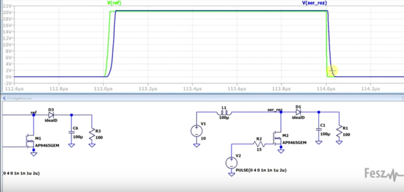
The other major piece of silicon in power supplies like this that drives noise are the switching transistors. Since the noise is generally caused by the switching itself, there is a lot that can be done here to help limit it. One thing is to slow down the amount of time it takes to transition between states, limiting the transients that form as a result of making and breaking connections rapidly. The other, similar to selecting diodes, is to select transistors that have properties (specifically relating to inherent capacitances) that will limit noise generation in applications like this.
Of course there is a lot more information as well as charts and graphs in [FesZ]’s video. He’s become well-known for deep dives into practical electrical engineering topics like these for a while now. We especially like his videos about impedance matching as well as a more recent video where he models a photovoltaic solar panel in SPICE.


When the subject at hand is noise, it strikes me as fortunate that the switching times AREN’T “actually zero”. The faster the edge, the higher the harmonic content. Sure, fast switches are more efficient – but they also generate more RF energy at higher frequencies.
I find that a fun thought experiment. At what point for getting switching times shorter/more square would a device necessarily be emitting gamma rays as harmonics.
“Switching” is modulating the current or flow of electrons in a circuit. That raises the question of “What does modulating current even mean, when the wavelength is smaller than an atom?”
I thought FesZ was mostly for RF and filter stuff but I am pleasantly surprised to find power electronics as well.
Another high recommendation for power electronics is professor Sam Ben-Yaakov
Well, if he’s coming from the filter/RF side, that explains the use of gate resistors. As an energy guy you try your best to minimize them. You choose a beefy gate driver (which is completely defeated by even a 15 Ohm gate resistor) and low gate capacitance FETs to get as steep as possible switching, and to keep the voltage spikes on the power side under control, you design low inductance current paths to the filter capacitors. This automatically reduces emitted noise. To get more efficiency (and lower noise) you leverage some resonances to get zero voltage switching or zero current switching.
If you f’d up the design and have no time to do another iteration, the gate resistors may buy you some db of noise by killing efficiency, but if you use them as the main part of your noise control, you may as well use a linear regulator.
The gate resistors can also be used to reduce the likelihood of oscillation and ringing. Yes, that’s mostly a problem in the analog realm, but it’s my understanding that it can also appear transiently in switching applications, showing up as ‘messy’ edges.
Carefully chosen ferrite beads on the gate leads can be a good compromise here. And whether you’re using resistors or ferrite, as you mentioned you need to pay close attention to gate capacitance. I wonder how many power supplies behave erratically after they’ve been repaired because that “exact replacement” MOSFET wasn’t exact enough.
If you want a really deep dive, MIT have put up their course 6.622, Power Electronics on You Tube. Here’s the first lecture from David Perreault, and another 37 follow that.
https://www.youtube.com/watch?v=f7oXhDatwtY
If you want to jump ahead, methods of soft-switching to reduce the switching spikes are discussed in lectures 33 and 34.
Can’t recommend these lectures enough.
Are diodes and switching component susceptible to age with time, and can this degrade the performances and increase noise? In other words, when repairing or restauring an old SMSP, is replacing diodes or switching driver should be considered?
I’m looking forward to how other folks here may answer your question. In my experience diodes, MOSFETs, and other semiconductors don’t really age unless they’ve been subjected to excess heat, current, or voltage – the latter includes static discharges.
It’s possible for just about any semiconductor to be damaged in such a way that its characteristics change, and/or it fails some arbitrary amount of time after the damage occurs. But in general, outside of what i might call “stress damage” they don’t age in the same way that capacitors and other passive components do. As far as I can tell…
Thermal cycles and humidity may cause ageing, too, where the thermal cycles have to be seen on die level (the heat transfer from die to case goes with the thermal gradient, so with a constant case temperature, a little conduction losses and lots of switching losses the die temperature jumps around a lot during normal operation); the cycles may cause crack propagation on bond wires and enclosure sealing, which in turn may start to allow humidity to creep into and degrade the silicon. The housing may also crack due to mechanical stress, so don’t bend the diodes legs too close to the glass body. That said, I haven’t yet heard of semiconductor ageing outside high performance circuitry (megawatt scale inverters…) as common problem, too.
I wouldn’t worry too much about that. I worked in applications engineering in the mid-1980’s in a place that made VHF and UHF power transistors, mostly for military radars and communications. I did not get involved with the wafer fab and certain details of they physics, only the application. When someone in the lab would have a tiny transistor putting out short pulses of hundreds of watts for a radar, the whine from the violent expansion and contraction cycle from the power pulses could be heard all over the lab, yet these things had a respectable lifetime. As for humidity, the dice (ie, the actual silicon chips) were passivated, which I understand is kind of like coating them with a few nanometers of glass.
Around 1993, I designed a Maxim switching-regulator IC into one of our products for aircraft. A couple of years after we had it in production, Maxim changed the process, making the switching edges faster, without telling us. Suddenly we had a whole batch of assembled PC boards that made a lot of electrical noise that was getting into the aircraft radios. We couldn’t afford to scrap the boards and take the time for a re-design, so we had to manually modify them by soldering capacitors directly to IC leads, with no lead length (because of lead inductance), and put ferrite beads over interface wires. Subsequent designs incorporated what I learned there, by adding SMT ferrite beads and an extra LxC filter at the output.