
LTSpice is a tool that every electronics nerd should have at least a basic knowledge of. Those of us who work professionally in the analog and power worlds rely heavily on the validity of our simulations. It’s one of the basic skills taught at college, and essential to truly understand how a circuit behaves. [Mano] has quite a collection of videos about the tool, and here is a great video explanation of how a bootstrap circuit works, enabling a high-side driver to work in the context of driving a simple buck converter. However, before understanding what a bootstrap is, we need to talk a little theory.
Bootstrap circuits are very common when NMOS (or NPN) devices are used on the high side of a switching circuit, such as a half-bridge (and by extension, a full bridge) used to drive a motor or pump current into a power supply.
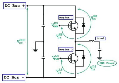
From a simplistic viewpoint, due to the apparent symmetry, you’d want to have an NMOS device at the bottom and expect a PMOS device to be at the top. However, PMOS and PNP devices are weaker, rarer and more expensive than NMOS, which is all down to the device physics; simply put, the hole mobility in silicon and most other semiconductors is much lower than the electron mobility, which results in much less current. Hence, NMOS and NPN are predominant in power circuits.
As some will be aware, to drive a high-side switching transistor, such as an NPN bipolar or an NMOS device, the source end will not be at ground, but will be tied to the switching node, which for a power supply is the output voltage. You need a way to drive the gate voltage in excess of the source or emitter end by at least the threshold voltage. This is necessary to get the device to fully turn on, to give the lowest resistance, and to cause the least power dissipation. But how do you get from the logic-level PWM control waveform to what the gate needs to switch correctly?
The answer is to use a so-called bootstrap capacitor. The idea is simple enough: during one half of the driving waveform, the capacitor is charged to some fixed voltage with respect to ground, since one end of the capacitor will be grounded periodically. On the other half cycle, the previously grounded end, jumps up to the output voltage (the source end of the high side transistor) which boosts the other side of the capacitor in excess of the source (because it got charged already) providing a temporary high-voltage floating supply than can be used to drive the high-side gate, and reliably switch on the transistor. [Mano] explains it much better in a practical scenario in the video below, but now you get the why and how of the technique.
We see videos about LTSpice quite a bit, like this excellent YouTube resource by [FesZ] for starters.


As a motorbike rider, I try to avoid low side and high side driving as the plague. :D
But this is what Hackaday is doing for me: as (digital) computer scientist, I am gradually learning about analog electronics and power supply design after all. ;)
I’ll second that, although I always feel as though I skipped a few grades in school when I read articles like this. And yet, slowly I learn!
Simulating a half bridge driver and analyzing how it works is a good thing. However, for a practical circuit, it’s more common to simply use a MOSFET driver IC for it. Such an IC provides:
High side and low side Fet driver (with peak currents upto 3A for fast switching).
Shoot though prevention with built in delays, so you can’t short circuit your half bridge due to for example a software fault.
Galvanic isolation.
These IC’s are very common, and used in all sorts of motor controllers, and you can also use them in synchronous SMPS circuits. An example of such an IC is the IR2102 (Cost EUR96ct each for 100+).
the IR2102 doesn have shoot through prevention nor does it have galvanic isolation …
It’s got a 600V insulation barrier between the logic inputs and the high side FET driver. But this is indeed not a complete isolation. You’re also right about shoot through prevention. Not present in IR2102, but IR2103 does have circuitry for dead time generation and shoot through prevention.
You’ll be interested (or alarmed..!) to know that these type of parts are not insulated at all.
In fact, HVICs are constructed with the high-side circuitry atop a thick, lightly-doped junction: hence the high standoff voltage, but this junction becomes forward-biased for Vs or Vbs < Vss. The junction can be subdivided of course, allowing HV MOSFETs to be built across the barrier; a pair, cascoded, serve for level shifting. Pulsed commutation is usually used, I believe, to save on quiescent current and power dissipation (since they draw from Vbs directly to Vss).
Newer families are available with 30V or more of transient immunity, in the reverse direction. Obviously(?), communication is unavailable during such excursion (the high side remains latched in its initial state before communication is lost, as you’d expect from a pulse coupling scheme). For higher voltages, true isolated types are required (which also indeed include true monolithic designs; TI’s capacitive-coupled and ADI’s inductive-coupled families are typical).
Aren’t PFETs just as good these days? I thought NFETs being lower Rds was something that was true maybe 10 years ago. Bootstrapping drivers are so much trouble, I just use PFETs on the high side, NFETs on the low side and implement dead time myself (in the code).
Then again, I do power electronics only as a hobby, and low power IIoT stuff professionally so my opinions are skewed
nfets are still better and cheaper and when you need to switch higher voltages gatedrive for a pfets gets just as messy
P Channel in high side and N channel on low sidevonly works when VDD is less than VGSmax; which is about 20V.
If you need higher supply voltages, you’ll More expensive P channel MOSFETs, or high side drivers.
No link to the .asc file?
I got extremely frustrated with using LTSpice or ngspice to model SMP. Runs were continually dying with transient issues. No doubt due to ignorance (other people use them), but a show-stopper for me. I’ve had much better success with Xyce, from Sandia National Labs. (It’s almost like they have a lot of experience modeling high intensity transients or something.) I think it’s also a lot smarter about calculating the time steps in general; usually it finishes in a fracton of the time that LT or ng take, with fewer steps, and just as accurate.
The downside is that there are some differences in the semantics and execution of the netlist dot commands, and sometimes for the device models themselves. Some models from the MicroCap libary (esp. older ones) won’t load. They’ve usually been fairly simple to patch. But you can’t just drop Xyce into KiCad as its built-in modeler.
Lockup or “timestep too small” is always a setup and modeling issue — though not always one that can be solved. Numerical solution is a notoriously difficult problem, after all.
The usual causes are:
– Degenerate nodes or loops (near-singular matrix; LTSpice’s default RSHUNT and CSHUNT settings usually avoid a fully singular matrix), caused by connecting capacitors in series without “bleeder” resistors, or inductors in parallel without DCR
– Unrealistic dynamics from poorly modeled (or wholly absent) parasitics (all real circuits have R, L and C, between all points — we must implement the speed of light in SPICE)
– Extremely dynamic (read: poorly modeled) active devices; for example any time you see a IF() statement in SPICE, it’s almost certainly a harbinger of shitty convergence. TABLE statements can be poorly used as well.
Favoring the smoothness brought by the application of continuous (including continuous N derivatives for N-order integration!) functions, and parasitics, a smoother solver usually helps, too (GEAR order 2+).
These all come at a price (slower integration), of course. A sufficiently advanced circuit can always find some incredibly tight and complex loop to grind into; this isn’t a well-defined problem. (An alternative solution suggests itself: don’t make pathological circuits in the first place! They probably don’t work well IRL either.)
Finally there are various parameters to adjust (fewer of these in LTSpice, but the classic 3f5/XSPICE set I know well):
– RSHUNT and GMIN address nonlinearity of the system;
– ABSTOL, VNTOL and CHGTOL affect numeric accuracy (it may be worth setting these to about RELTOL times the smallest expected respective amount/change in the circuit);
– TRTOL is how fast the integration adjusts to nonlinearity (i.e. how sharply timestep is increased or reduced to account for increasing error);
– RELTOL is a general (relative) tolerance; lower is more precise, but will take longer to run; larger will produce chunkier waveforms and show poorer stability/accuracy (stability in terms of energy conservation; an RLC circuit’s Q factor for instance);
– ITL4 is the Transient iteration limit; you’ll need to specify higher value in more complex circuits.
– And, for Transient Analysis, set initial and maximum timestep respectively. If you want to keep smooth, well sampled waveforms, consider reducing maximum timestep.
Thank you! The notes about parameters are especially helpful. This would make a great series of posts for HaD or your blog.
Hand-crafting a bootstrap driver isn’t the most useful thing, overall, but it’s good fundamentals, and might even come in handy for a quick breadboarding when something simple needs lashing up and driver ICs aren’t to hand. Last year, I ran through a few discrete design exercises that readers may find of interest (I would also encourage building and running the simulations!):
https://hackaday.com/2024/10/13/building-an-automotive-load-dump-tester/
In particular, this part: https://www.seventransistorlabs.com/Articles/Hysteretic.html#exp
Between this and part 3, the choice between bootstrap and isolated drivers is also discussed. The circuit is still (mostly) discrete, using a few more transistors, but with much improved functionality.