Over on his blog our hacker [Scott Baker] has a Magnetic Bubble Memory Mega-Post.
If you haven’t heard of magnetic bubble memory before it’s basically obsolete nonvolatile memory. Since the 1970s when it was introduced this type of memory has been outperformed in every dimension including durability, reliability, price, density, performance, and so on. For any given application of bubble memory you will be able to find an alternative technology which is better in many ways. Except if you want some old tech to geek out over, in that case magnetic bubble memory is for you!
In his article [Scott] begins by introducing the Intel 7110 Bubble Memory branded variously as “Intel Magnetics” and “Memtech”. These chips are marked up with what [Scott] explains are a defect map. The defect map is for indicating which storage areas are defective so they can be avoided. This map is printed atop the package and also stored in the bubble memory itself. [Scott] says the engineering samples have the defect map set to “FF”, but it’s not clear if that means “defective” or “not defective”. If you know, please do enlighten us in the comments!
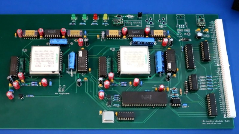
In his fascinating and detailed notes [Scott] goes on to discuss various multibus boards, which can integrate multiple memories; and multimodules, which can plug in to multibus boards. [Scott] shows off photos of clone multimodules and boards he made himself. He goes on to discuss HP 98259 bubble memory boards, the Memtech bubble memory cassette system, the Allen Bradley 8000MBC bubble memory cassette, Heathkit H8 bubble memory boards, and our favorite Scott’s Basic Bubble Computer. We have discussed magnetic bubble memory here on Hackaday before in articles such as Magnetic Bubble Memory Brought To Life On Heathkit and Magnetic Bubble Memory Farewell Tour.


I actually developed a product using the Intel 7110 when it was very new, so new that Intel still owned them, and if we stopped using them, they had to be returned. Imagine our surprise when we discovered that at about -6 deg C all the bubbles wandered off. You still had all the ones and zeros, but you didn’t know which loop they were in. Intel’s suggestion was to keep refreshing the entire array and the heat generated by the various electromagnets would keep all the bits where they should be. I still have one of the Garnet “chips”, and under a good microscope you can see the transfer gates and the minority and majority loops. Luckily SRAM was just around the corner.
He should do a post on “How I Found Out What FF Means” instead of asking the reader since he actually physically possesses the thing.
I will see if I can get in touch with him to ask the question.
Per datasheet, the 7110 modules have 1,048,576 bits of usable storage, and 1,310,720 bits of “gross capacity”. The difference allows for some known defects to exist in the module and still meet its usable storage requirement. “FF” means all loops for that entry are good. Grabbing one of my actual working modules, from a NOS sbx-251 module I bought on eBay a few years ago, the map reads “BFFBBBBBFBBFFBFBBFFBBBFDDDD5DDDFDDDDDFFFFF7FFFB…”. When you see a F, that in binary is 1111. B is 1011, D is 1101, etc. If we assume most of the loops in the bubble are good, then we could logically guess that the zero bits are defective loops and the ones are good loops. All of my working samples, even NOS memtech samples that were late in the manufacturing lifecycle of bubble memory, have at least a few digits that are not “F”. Based on experience, it seems unlikely any would have all Fs, which leads me to believe those two were just engineering samples, not initialized and not intended for production use. Oh, and thank you Hackaday for featuring my page. :D
Thanks Scott!
mutlimodules? Spell check? :D
lol. Nice catch. I will fix that up, thanks.
Sandia labs used bubble memory to fuze ground-based nuclear weapons.
Rekeying required entry of a passcode. Limited tries only allowed.
Bubble memories became corrupted.
Failing nuclear weapon had to be sent to Pantex for repair … at ~$500,00 per fix.
My dad, John Ypma, worked in the area of bubble memory at Rockwell. I was a child and bubble memory was certainly a household name. I remember hearing the name Andy Bobeck. I recall it as an exciting time with my parents going to Europe for conferences and then a very disappointing time. It was very interesting to me to see bubble memory still being discussed!
Bubbles were like CCD memory back then. Just on the cusp of being practical, but never quite getting there. They needed a density of 4 to 1 over RAM and maybe 2 to 1 is all they ever got.
And then EPROM tech begat flash and the game was over.
There is a good video on the retro collective on this type of memory used in an arcade board.