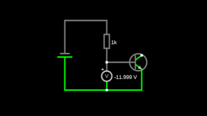
For our 2025 Component Abuse Challenge there have been a set of entries which merely use a component for a purpose it wasn’t quite intended, and another which push misuse of a part into definite abuse territory, which damages or fundamentally changes it. [Ken Yap]’s use of a transistor base-emitter junction as a voltage reference certainly fits into the latter category.
If you forward bias a base-emitter junction, it will behave as a diode, which could be used as a roughly 0.7 volt reference. But this project is far more fun than that, because it runs the junctions in reverse biased breakdown mode. Using one of those cheap grab bags of transistor seconds, he finds that devices of the same type maintain the same voltage, which for the NPN devices he has works out at 9.5 volts and the PNP at 6.5. We’re told it damages their operation as transistors, but with a grab bag, that’s not quite the issue.
We’ve got a few days left before the end of the contest, and we’re sure you can think of something worth entering. Why not give it a go!


Erm…a diode you mean?
A very unstable, unrepeatable voltage reference that is worse than Zener diode. Not only the breakdown voltage increases with temperature, but is also dependent on current and characteristics of a particular transistor. There’s a reason no one uses them as references. Also, quantum noise, which is often used in RNGs and noise sources.
There’s a reason no one does anything the way described in the stories submitted to this challenge. That’s kind of the whole point.
Isn’t the point of challenge to get something USEFUL from the abused component?
This reference, frankly, is not useful.
I once designed a dual channel DDS generator, with the idea of overclocking the main chips to 100MHz because that would extend the available frequency range at a cost of some additional losses, heat and higher noise and harmonics beyond the range. I also overclocked a PIC microcontroller just to see, what would happen. It ran faster. That’s useful, too. I’ve also seen somewhere a stereo headphone amplifier made of two TL431s. I even built it p2p style, and it worked very well. That’s a legit component abuse – going beyond the part’s parameters or applications.
Taken literally, it just means abusing components.
It could also be psychological or verbal abuse.
I used a reverse bias 2n2222 in a little solar application to move my plants around on a turntable. Was a sharper transition than the zener i had as the current Was getting soaked up in the zener knee waiting to kick over when the panels weren’t quite powerful enough. It’s lasted a few months of use so far without blowing up. Not a good use, but a practical one.
There’s a nice collector-base diode with a negative TC in series with that positive TC reverse biassed base-emitter diode. Choose the right device type, do some sorting, and the TCs cancel.
This was a lab project in my undergrad!
Build a wind anemometer with no moving parts.
Most of us tried to measure the forward Vbe changes with wind on the transistor, but the changes were so small, they were hard to separate from the noise. The desired solution was to operate in breakdown because the reverse Vbe changes significantly larger with wind speed, than the forward Vbe.
please describe in detail. interesting!
More importantly, since the breakdown voltage is much higher, there is a greater self-heating effect on any amount of current that flows through, which makes it possible to detect wind (convection heat loss) rather than just ambient temperature in the first place.
That’s the basic principle of how hot wire anemometers work. Current causes heating, wind causes cooling. Temperature changes the resistance of the wire. When you measure the wire resistance and ambient temperature, you get the power loss from the wire and difference in temperature, and can correlate that with different wind speeds.
That was used in every dbx product when they were made from discrete transistors. I worked there starting in 1971.
Apparently, the use of any BJT in base-emitter reverse-bias breakdown mode damages the device for use in normal forward-bias mode by decreasing current gain and increasing leakage. I have been unable to find a physical reason for this action that covers all BJTs.
For any BJT, allowing too much current to flow in reverse bias mode might result in localized or widespread heating, disrupting the crystal structure or allowing rediffusion of dopants. But if current is limited? …
For planar BJTs, the explanation proposed is that the “hot” electrons create recombination sites (traps) between the silicon and the silicon oxide. I assume that once again disrupting the crystal structure is to blame.
What about grown-junction and alloy-junction BJTs? (Were these only germanium?) The active regions are buried; they can be (I think) constructed without any place for traps to form in an oxide interface. If so, and degradation still occurs, what’s the mechanism? The same question applies to BJTs that are not passivated.
Does anybody have good knowledge of this?
Don’t know, but there’s an old 73 article on modifying a transistors characteristics by running them in different situations like this
So basically a Temperature Controlled Voltage Reference TCVR.
Choose the desired voltage by increasing or decreasing the heat
would it be possible in this mode to detect alpha beta or gamma radiations?
I saw (and tried) a one-transistor circuit that’s blinks an LED. It uses the breakdown voltage of CE by hooking up an npn transistor backwards. The base is left floating. It oscillates and provides nice short pulses when run at 9v – 12v. I tried it and it does work.
Reminds me of when we managed to get a triode valve running backwards.
Didn’t last long.
People here saying how bad it is should look into how this was actually used in devices. The vfo in a Heathkit HW-101 transceiver uses it. Only transistor in the whole transceiver
This was a “practice” in old days when there was not so many Zener diodes around. If the current “workpoint” of the inverse polarized EB junction is the same as direct polarized (0.1mA max) it will not destroy the transistor, but it is a very “weak” Zener diode, when compared to real one.