[Andrew Greenberg] has some specific ideas for how open-source hardware hackers could do a better job with their KiCad schematics.
In his work with students at Portland State University, [Andrew] finds his students both reading and creating KiCad schematics, and often these schematics leave a little to be desired.
To help improve the situation he’s compiling a checklist of things to be cognisant of when developing schematics in KiCad, particularly if those schematics are going to be read by others, as is the hope with open-source hardware projects.
In the video and in his checklist he runs us through some of the considerations, covering: visual design best practices; using schematic symbols rather than packages; nominating part values; specific types of circuit gotchas; Design for Test; Design for Fail; electric rule checks (ERC); manufacturer (MFR), part number (MPN), and datasheet annotations for Bill of Materials (BOM); and things to check at the end of a design iteration, including updating the date and version number.
(Side note: in the video he refers to the book The Visual Display of Quantitative Information which we have definitely added to our reading list.)
Have some best practices of your own you would like to see on the checklist? Feel free to add your suggestions!
If you’re interested in KiCad you might like to read about what’s new in version 9 and how to customize your KiCad shortcut keys for productivity.


we definitely could use a Strunk & White of schematics.
my small ask of the world is that when schematics are rendered into pdf, please provide a monochrome rendering fromthecadpackage* (which knows what are marks and what are background). dithered colors on a laser printer are unreadable; all the more so reduced from a B-size schematic to A-size paper.
Good point on the color. I don’t know why it’s acceptable to put all manner of helpful color coding on a schematic, but then, only the engineering department “needs” a color printer. Apparently, assemblers and testers are expected to just deal with faded, near-illegible markings or somehow use a laptop screen to follow traces across five non-sequential pages of a 40-page schematic.
It’s been decades since I have printed a schematic
ohh… that’s sad. Perhaps tomorrow or the day after that, eventually you’ll have one printed, no worries, your time will come.
You’ve clearly never worked on anything large or complex, or something that’s not on the bench next to a computer. Printed schematics are a “godsend”.
Haven’t watched the video yet, but alongside this comment, can people stop splitting the schematic into a billion fragments and then putting them all on the same page anyway. It’s a horrible trend that just makes it harder to read, and adds nothing.
Appendix B of “The Art of Electronics” by Horowitz and Hill is a good start.
Appendix B in the Third Edition. It’s Appendix E in the Second Edition.
As someone who highlights signal paths on a schematic – I’ve been making do with Photoshop /Affinity for years.
Adding a second, thick green /orange /whatever line to RF, IF, AGC etc. paths.
Need to recheck on Kicad features: I have a circuit right now, that could do with some oscilloscope waveform pictures.
I’ve always been obsessive about schematics having flow, being uncluttered, and being readable at a glance. That applied when I was still drawing them by hand, and it applied in spades when I could drag, drop, and route connections without grabbing an eraser.
Sometimes I would even have PCB design in mind while drawing the schematic, so the schematic to some extent mirrored the final PCB layout. I’m also obsessive about clean PCB layouts – trace lengths, grounding considerations, etc. come first; but immediately after that comes a balanced, logical, and pleasing layout.
And I thought all of the above was just the excessive nit-pickiness of my specific flavour of ADHD. It’s good to know that it was the kind of thing that others find real value in.
I’ve always been bugged by poorly drawn schematics, especially when I’m troubleshooting. It’s hard enough to keep mental track of readings, scope traces, settings, and what I have and haven’t tried. Figuring out a schematic that seemed to have been drawn by a squirrel caching nuts around a forest was just a cause of unnecessary extra stress and confusion.
“Figuring out a schematic that seemed to have been drawn by a squirrel caching nuts around a forest…”
That applies to any kind of specification.
Could someone remove all the short circuits running through modern diodes.
There is no line through the official symbols so why do so many have one nowadays?
The IEC standard specifies a non filled area with a line through the symbol.
I’ve done a couple of KiCAD designs, and I’m very impressed with it. Schematic style is a whole ‘nother thing, and very much individual. The important thing is: can they be used by someone else to figure out how your circuit works and how to fix it.
Sometimes these ‘schematics’ are little more than an annotated illustrated parts list. It’s easier/quicker to label a connection rather than draw it. It’s not easy to see how many parts are connected especially with the wishy washy colours used coupled to the microscopic fonts which are then stored as a bitmap.
Draw all connections, use black on white and save as PDF.
If you have multiple sheets, try and lay the sheets so they can be pretty much taped together to form one large sheet.
Simple really.
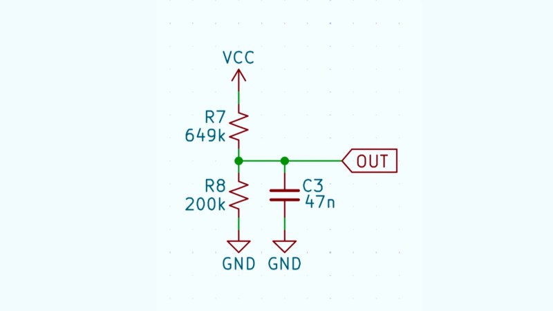
Why is OUT drawn as an input in the schermatic?
Thanks for mentioning that, I thought I was the only one having problem with that. If it’s an output why the wrong arrow direction. If it is an input connected to something names OUT then why is it on the right side of the schematic. Very confusing indeed, it does set the tone for the subject though.
I think in KiCad that is what’s called a “Global Label” and I don’t think they have a “direction”… it’s just a label for a point. You were expecting something else?
Missing from the checklist: 4-way junctions should never cross at right angles with a dot, that can be forgotten, or misread on a poor print. If you MUST have a 4-way junction in a small space, two of the lines (preferably minor circuits, not power buses) should be angled, and each will then join the common line with its own dot. This was always a rule with hand drawn circuits, but seems to have been forgotten nowadays.
Not:
|
—o—
|
but
|
/
–o—-o–
/
|
The only other valid cases I can think of where diagonal are acceptable wires are bridge circuits and multivibrators.
Aaargh! The Hackaday editor has removed leading spaces from my vertical and diagonal lines. You will have to imagine them, sorry.
We use diagonal connectors (very rarely) to show a common ground point where potentially local ground groups are joined, like where analog and digital grounds finally connect.
And yeah, I preach the please don’t have X connections make them Z or something to all the people I mentor.
What is missing is a way to create a text file that can be read by kicad to produce a schematic. I don’t care if it wires everything up, named connections are fine. Using a GUI to create a design is not in keeping with EDA principles. Realize we do not use schematics to design FPGAs or chips.
This Information really needs to be more widely disseminated amongst makers and open source projects. So many times I’ve just been utterly confused by a schematic not understanding basic building blocks because someone decided to break every convention in schematic layout.
Making readable schematics seems to be a lost art. I’m an EE and in my expericance the readability of most modern schematics is abysmal.
Admittendly part of that is due to the proliferation of huge chips with a million pins. But also
I have 3 pro tips. 1. Put a LOT of notes in your schematic, why things are there, what voltage ranges are expected on various wires, etc. Thank me later. 2. Give each component a requirement field and use it. This is extremely useful 5 years later when a part is out of stock or obsolete, and you can’t remember what the critical parameters are. 3. Don’t get too crazy with “just in case”/DNP parts. They clutter the schematic and make it hard to follow, and its not that hard to bodge parts on there if you need to even without a footprint.
The vast majority of people who draw schematics as part of their job draw them properly. The increase of bad schematics is fueled by how low the entry bar has become to draw a schematic and make hobby PCBs.
I see in quite a few forum posts asking to review schematics/layouts designed by ChatGPT where you can see nonsensical connections. That is scary.
Oh, wait… so I wasn’t SUPPOSED to be able to recognize simple textbook circuits instantly and without effort when the component symbols are arranged and traces ran in some weird, totally doesn’t match any textbook sort of way?
All these years I thought it was something wrong with me. Thank you!