When AI is being touted as the latest tool to replace writers, filmmakers, and other creative talent it can be a bit depressing staring down the barrel of a future dystopia — especially since most LLMs just parrot their training data and aren’t actually creative. But AI can have some legitimate strengths when it’s taken under wing as an assistant rather than an outright replacement.
For example [Aarav] is happy as a lark when birdwatching, but the birds aren’t always around and it can sometimes be a bit of a wild goose chase waiting hours for them to show up. To help him with that he built this machine learning tool to help alert him to the presence of birds.
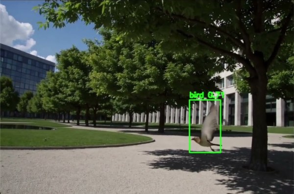
The small device is based on a Raspberry Pi 5 with an AI hat nested on top, and uses a wide-angle camera to keep an eagle-eyed lookout of a space like a garden or forest. It runs a few scripts in Python leveraging the OpenCV library, which is a widely available machine learning tool that allows users to easily interact with image recognition. When perched to view an outdoor area, it sends out an email notification to the user’s phone when it detects bird activity so that they can join the action swiftly if they happen to be doing other things at the time. The system also logs hourly bird-counts and creates a daily graph, helping users identify peak bird-watching times.
Right now the system can only detect the presence of birds in general, but he hopes to build future versions that can identify birds with more specificity, perhaps down to the species. Identifying birds by vision is certainly one viable way of going about this process, but one of our other favorite bird-watching tools was demonstrated by [Benn Jordan] which uses similar hardware but listens for bird calls rather than looking for the birds with a vision-based system.