Full Teardown Of A 2026 Amazon Fire Stick HD

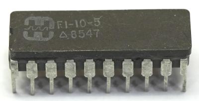
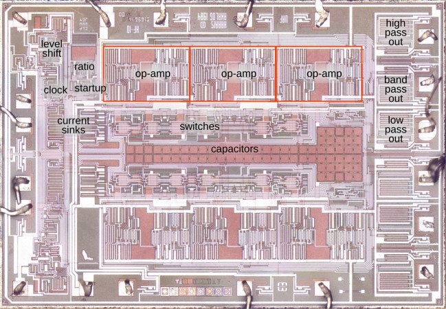
Die of the Amazon Fire Stick HD (2026) PMIC IC. (Credit: electronupdate, YouTube)

After the release of Google’s Chromecast so-called ‘streaming sticks’ have remained a popular form factor, even though such technology is these days part of ‘smart’ TVs. Being curious as to what kind of hardware they put into these sticks or dongles these days, [electronupdate] decided to do his typical full teardown of a 2026 model Fire Stick HD from Amazon, including the typical nekkid die shots.

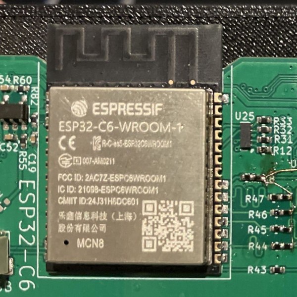
Although most of the bits inside are fairly typical, being just your typical Mediatek-sourced solution, the ceramic patch antennas for Bluetooth and Wi-Fi are a rather interesting detail, as are the purported limitations that make this the ‘HD’ version of the Fire Stick, unlike its 4K brethren.

The used Mediatek MT8698D SoC isn’t so different from the SoC in those 4K versions, with the 2025-era 4K Plus using the MT8696D, but the 4K Select using basically the same SoC as the HD version, featuring the same G310V2 GPU at 500 MHz per the Amazon Developer documentation and the same decoder block (VPU), both of which are capable of 4K video decoding. This implies that the HD vs 4K distinction is purely software-based.

The Amazon Fire Stick HD PCB devoid of its metal shielding. (Credit: electronupdate, YouTube)

After popping open the device and noting the various ICs, the NAND Flash, the Mediatek MT7902 wireless IC, the PMIC and the aforementioned SoC all have their caps popped in order to take a closer look at their dies. For reference, as one of the largest ICs, the SoC die is a mere 5.2 x 6.45 mm. The PMIC die is more interesting as usual, as this one integrates USB-PD functionality, adding quite a bit of logic to what is otherwise a fairly mundane bit of power management features.

Overall not a very surprising design, though it does tickle that thought in the back of one’s mind whether it could be turned into a ‘4K stick’ with a few software tweaks, or perhaps more simply by installing plain Android onto its 8 GB of eMMC.

Continue reading “Full Teardown Of A 2026 Amazon Fire Stick HD”

A USB Port By Any Other Color…

[Dr. Gough] bought a generic USB 3.0 hub on an Asian website. Surely, USB 3 is mature enough that even the cheapest hub will have some IC in it that will work well, right? You’d think so, but a little exploratory surgery showed that the only thing about this hub that was USB 3 were the blue port connectors.

We have a few problem USB hubs ourselves, so it might be worth doing this to any you have lying around. The first clue: most of the connectors on the PCB only have four pins. On closer examination, the hub appears to be a USB 3.0 extension cable with a USB 2.0 hub made from two HS8836A chips.

Not only are these USB 2-only, but all the ports on an HS8836A also share the same USB 1.1 bandwidth. Some hubs can provide multiple ports full 1.1 bandwidth, using the higher-speed USB protocol to the PC as a backhaul.

Continue reading “A USB Port By Any Other Color…”

A Look Inside A 1997 BBC Ceefax Generator

Ceefax was the BBC’s broadcast teletext service that ran until 2012, providing text and rudimentary graphics that were broadcast invisibly with the TV signal. In order to get this teletext data merged into the analog TV signal, special equipment was needed, of which [Nathan Dane] has a 1997-era unit on his bench to take a gander at.

Interestingly, until this time the Ceefax signal had been generated centrally in London, meaning that regional TV broadcasts might have Ceefax issues on occasion due to retransmission glitches. This makes this Ceefax Inserter  system so much more interesting, as it was one of the early examples of what these regional stations would end up installing in their racks.

At their core these units are regular PCs, running MS-DOS 6.22 on a 486-class CPU and all the typical bits and bobs that go with a PC. The speculation here is that these are essentially rebranded industrial PCs, which would make a lot of sense. As for how [Nathan] got his hands on these units, it required a deal with the company scrapping them, preventing him from showing details of the software configuration.

Following a booting demonstration, we get the teardown of a typical 1990s rackmount PC, revealing a rather interesting backplane with the mainboard being one of the cards on it. Of these, two ISA cards provide the special Ceefax sauce as well as a timing signal in the form of a PDC card featuring a Lattice CPLD or FPGA that VCRs could use to automatically start recording.

The Ceefax main event comes in the form of the inSERT Teletext Encoder card. This is pretty much its own computer system, featuring a TI TMS34010 CPU and its own RAM as well as IO. Compared to modern takes on teletext generators, this card appears to directly mix the analog signals, without any kind of conversion.

Although teletext systems have been largely shutdown now at this point due to the transition to digital TV broadcasting, there’s still a lot to be said for having such a service available for basic news and information.

Continue reading “A Look Inside A 1997 BBC Ceefax Generator”

Breaking Into A Prison Tablet

Usually the term ‘jailbreaking’ isn’t meant to be taken quite that literally, but in the case of the US prison tablet that [Hugh Jeffreys] got sent, it’s really quite apt. Unlike the typical transparent prison electronics, this tablet is hermetically sealed inside an opaque plastic case, with the Windows 10 install firmly locked-down and not allowing anything more to be done with it than access some prison-provided services via the browser in kiosk mode.

The first challenge was to see whether it could be booted at all, with just four metal pads visible on the side of the case. These turn out to correspond to USB pins, but the tablet only briefly tries to turn on with a charger connected. This means that a teardown is required, which ended up involving a hacksaw due to the sealed case.

Inside the case is the Windows tablet with the back cover removed, presumably for easy access to extend its USB port. All of this is embedded in foam and more gunk that makes disassembly rather messy. With the case opened it becomes clear that the likely reason why this tablet was junked was due to a bad third-party charger board, as using the tablet’s own USB port it charges happily and even turns on.

From there it’s a bit of a fight with the locked-down Windows installation, but as it’s just a Windows 10 Home installation, there’s no drive encryption or such to get in the way. This allows for the device to be fully jailbroken, revealing its specifications as an Iview Optimus-C-8001, powered by an Intel Atom Z8350 at 1.44 GHz with a blistering 2 GB of RAM. The Windows installation was from 2018, with apparently no updates since.

Despite the very high school arts-and-crafts appearance of the case itself, the tablet itself isn’t too shabby considering the limited hardware specifications. Although getting the case off is a bit of a pain, it’s not a bad catch if you can find one of these puppies in the e-waste bin.

Continue reading “Breaking Into A Prison Tablet”

Autopsy Of A Freshly Cooked 10Gbit SFP+ Network Adapter

With the advent of affordable 2.5 Gbit, 5 Gbit, and 10 Gbit consumer networking gear, more and more people are taking advantage of these higher networking speeds, with [This Does Not Compute] having used 10 Gbit SFP+ modules over regular Cat-5e copper to connect to a NAS in the next room. Only problem was that after a while these SFP+ modules began to start dropping frames. On taking a closer look at these modules, he found that they were running pretty hot: 40°C while idle. A teardown of one of these modules showed severe discoloration due to heat.

Side view of the SFP+ module's PCB. (Credit: This Does Not Compute, YouTube)
Side view of the SFP+ module’s PCB. (Credit: This Does Not Compute, YouTube)

Inside these 10Gbit modules is the Marvell-branded Alaska X 88X3310/40P PHY, which despite the ‘low-power’ claims have a metal heatsink glued onto the actual IC and thermally coupled to the module’s metal enclosure. The other side of the PCB was quite discolored, further indicating how hot these modules run in operation. Some digging revealed that this can go up to around 2.5 watts.

Perhaps the most fascinating part of this teardown is the discovery of an 8051-based MCU that’s responsible for telling the switch the module is put into that it is a 30-meter multi-mode fiber module, presumably for compatibility purposes. It’s definitely an interesting feature of these FS-branded SFP+ modules.

These old modules were replaced with Wiitek-branded modules that are supposed to use only up to around 1.5 watts in operation courtesy of a newer chipset, in the hope that these wouldn’t fry themselves. At idle these do however still run at 30 °C. As noted in the comments, it might be a good idea to have active airflow over high-speed networking gear like this, as they generally can get pretty hot and sometimes crispy.

The final solution for the video’s networking problem was to just run single-mode fiber to the room and use appropriate SFP+ modules for that, also because these run noticeably cooler. If you still have room in your cable ducts, that would seem to be the optimal solution.

Continue reading “Autopsy Of A Freshly Cooked 10Gbit SFP+ Network Adapter”

The Repair Nightmare That Are Smart Rings

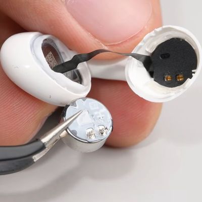
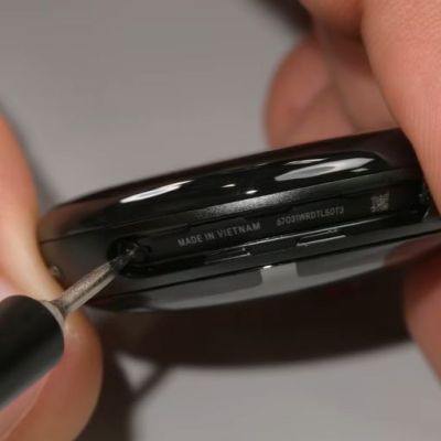
In the quest to make every wearable device ‘smart’, a lot of electronics along have to be crammed in very small spaces, along with ways to make them resistant to environments that our bodies do not mind, like getting hit by a rainstorm or simply washing our hands. These two factors combined make especially devices like smart rings an interesting case study for repairability, with [iFixit] recently taking apart a modern Oura smart ring to assess its e-waste factor after the built-in battery dies.

The tiny 10.5 mAh Lipo cell in the Oura Ring 5. (Credit: iFixit)

The subject of the teardown video is the Oura Ring 5, a $400 smart ring that’s designed to track your vitals much like a wrist-worn fitness tracker — just in a much smaller package. This metal-and-epoxy sandwich can definitely survive a good rain shower and washing of hands, but to get to the internals rather forceful methods were needed, unlike previous Oura and Samsung smart rings where some applied heat was enough.

In the Ring 5’s case even more heat was needed to make the inner ring start to slide out, but by that point the Li-ion battery inside had already popped from the heat. The inner ring then got stuck and more violence was required to continue the disassembly and get to the super-tiny, 10.5 mAh battery. Of course, at this point the smart ring really won’t be getting back together, never mind still work or be waterproof, which is a central issue with these smart rings.

With the EU’s February 2027 deadline for user-replaceable batteries looming on the horizon, it’ll be interesting to see whether devices like this can squeeze into an exception category, or whether manufacturers will have to massively redesign or stop selling these devices to this rather large market. So far this particular regulation has already forced Nintendo to make a special Switch 2 console for the EU.

Continue reading “The Repair Nightmare That Are Smart Rings”

Learning About Ground Loop Isolators Thanks To A Scam Product

When [Denki Otaku] bought a ¥1,200 (roughly €6.5) XLR ground loop isolator off Japanese Amazon, he initially didn’t suspect that anything was off. Since they’re fairly simple devices, with basically a 1:1 transformer per channel in some kind of enclosure, the price wasn’t unreasonable.

That’s before a teardown showed that this ‘ground loop isolator’ actually contains direct wiring between the XLR sockets, but that doesn’t mean that you cannot still make an educational video about the real devices.

First the basic theory is explained, before the fake ground loop isolator is subjected to an analysis, showing why you’d want to use the real deal. Of course, detecting a fake one is pretty easy, as a simple continuity test with a multimeter  or similar will show that DC passes right through the fake isolator.

Next a real ground loop isolator was designed with a custom PCB and a high-pass filter added to the feature list. Here rather than a very basic filter with cheapo parts there was definitely some gold-plating going on, but it does show what you can do in addition to just adding a few simple transformers for ground isolation purposes.

The finished ground loop isolator device is pretty large, and would definitely require a larger enclosure than the homeopathic device, but it makes for an easy test bed with convenient access during the subsequent analysis.

Here each of the two channels has its own transformer and filter, with an initial test just by ear making the injected 2 kHz noise signal appear to go completely away.

Next, an oscilloscope is used to visualize the functionality, with the non-isolated 440 Hz test signal first shown with and without the injected noise, showing the clear impact of the noise and subsequently the isolator.

Of course, high-frequency noises will still pass through the transformer via parasitic capacitance leakage between the windings, so it’s not a silver bullet. Here the analysis at the end of the video shows the noise-rejection characteristics of these isolators, and why adding a high-pass filter makes a lot of sense. Finally, the scam device’s XLR connectors were reused in an enclosure for this custom board, giving it some purpose after all.

Continue reading “Learning About Ground Loop Isolators Thanks To A Scam Product”