Processor design over the last few decades has moved toward RISC processors that aim to implement a few simple operations very efficiently. For a while, though, the trend was toward ever-more-complex CISC designs that let programmers implement complex behaviors using as few instructions as possible. Few processors took this approach further than the Intel iAPX432. This hyper-CISC processor was a commercial failure, largely due to its notoriously poor performance, but [MarkTheQuasiEngineer]’s benchmark suggests that this notoriety wasn’t totally deserved.
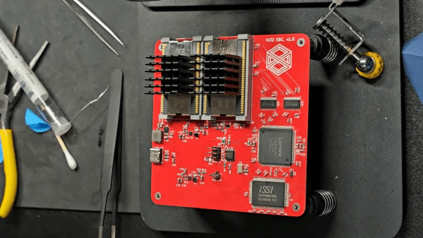
The first step before running a benchmark was to build a computer around the processor. The iAPX432 was implemented in three chips, two of which acted as the general data processor (GDP), and one of which handled input and output. [Mark] built an SBC (design and code here) that houses the two GDP chips and an FPGA for I/O. The 432 did have a well-deserved reputation for efficiently turning electricity into heat, and the original voltage regulator failed rather quickly.
The 432 was designed to use machine code which was almost a high-level language, with built-in object-oriented programming. It had over 200 operators, some of which implemented complex object-oriented operations, and a wide variety of data types, but it had no directly-accessible general-purpose registers. In addition to the lack of registers, it also had a very complex addressing system, allowing both direct and indirect addressing. For better performance, [Mark] used direct addressing.
For the benchmark, [Mark] implemented the Spigot algorithm to calculate the value of Pi. The results were somewhat surprising: calculating 2048 digits, it beat his previous retro-processor benchmarks; an Intel 8086 running the same algorithm took 2.5 times as long. Based on the results of this hand-written code, [Mark] speculates that the 432’s poor performance had more to do with poor compiler optimization than with the fundamental design.
We’ve covered some of the history of this troubled chip before. For a similarly ambitious but ill-fated Intel project, check out the history of Itanium.


