 In a recent video [QWZ Labs] demonstrates an interesting technique to use 3D printing to make creating custom PCBs rather straightforward even if all you have is a 3D printer and a roll of copper tape.
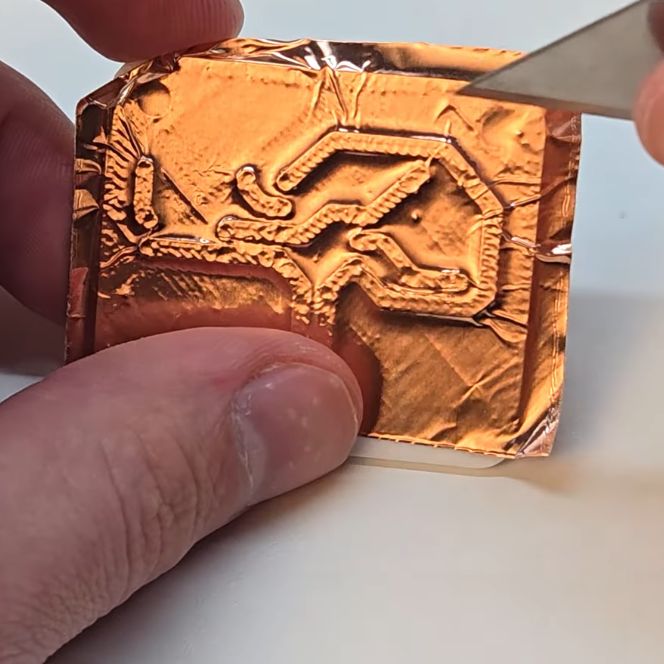
The PCB itself is designed as usual in KiCad or equivalent EDA program, after which it is exported as a 3D model. This model is then loaded into a CAD program – here Autodesk Fusion – which is used to extrude the traces by 0.6 mm before passing the resulting model to the 3D printer’s slicer.
By extruding the traces, you can subsequently put copper tape onto the printed PCB and use a cutting tool of your choice to trace these raised lines. After removing the rest of the copper foil, you are left with copper traces that you can poke holes in for the components and subsequently solder onto.
As far as compromises go, these are obviously single-sided boards, but you could probably extend this technique to make double-sided ones if you’re feeling adventurous. In the EDA you want to use fairly thick, 2 mm trace width with plenty of clearance to make your copper cutting easy, while in the slicer you have to check that the traces get printed properly. Using the Arachne wall generator option for example helps to fill in unpleasant voids, and the through-holes ought to be about 1 mm at least lest the slicer decides that you really want to drill them out later by hand instead.
While soldering is pretty easy on copper tape like this, desoldering would be more challenging, especially with hot air. In the video PLA was used for the PCB, which of course is rather flexible and both softens and melts easily when exposed to heat, neither of which make it look very good compared to FR4 or even FR1 PCB materials. Of course, you are free to experiment with whatever FDM, SLA or even SLS materials you fancy that would work better for the board in question.
Although obviously not a one-size-fits-all solution for custom PCBs, it definitely looks a lot easier than suffering through the much-maligned prototype perfboards that do not fit half the components and make routing traces hell. Now all we need is the ability to use e.g. targeted vapor-deposition of copper to make fully 3D printed PCBs and this method becomes even easier.


Kinda…silly!
If you’re making circuit boards that simple, use MDF or something and paste strips of copper tape on it.
Or better draw your circuit on a copper clad board with a permanent marker, and then etch it. Don’t even need to open kicad
Pretty sure its a proof of concept. 🙄
It is, but it’s still silly. I could see some applications where traces could be laid out on curved surfaces of some kind of embedded circuit doo-dad with blinkenlights. You could maybe even embed a circuit in-between layers, using a pause action and spending 10 minutes or so slowly carving out fiddly bits of tape, followed by a thick follow-up layer to take up the space created from the slightly embossed copper trace (stencil?). It still feels impractical, but this could work for those weird edge cases.
Essentially, it’s a slight twist on classic gold lettering used to make fancy initials in manuscripts. Glue is placed onto the paper, golden foil attached, let dry up and then the unglued gold is brushed off. It’s usually taught in calligraphy classes.
And if you then want to make it professional, flex PCBs with adhesive backing cost a few bucks on JLC and other eastern fabs.
This ^^^^ takes less time, can use toner transfer also.
Roll conductive paint and put copper donut stickers for soldering might work. Save on the cutting. Also conductive 3d filament is available. Got me thinking.
Etching is always messy and smelly so while looking cleaner is not really comparable.
The main benefit of 3d printing is that the board could be structural. Just ptint the walls of a box together with the pcb, just need enough clearance to squeeze the components in later.
H2O2 + Vinegar + Salt is actually very clean and only as smelly as vinegar, which is not too bad.
And citric acid (cooking ingredient) does not smell at all and has even better electrochemistry.
Every time I have tried the permanent marker trick the ink starts to wash off before the copper is etched through. I have obtained functional boards this way but only very simple ones and even then the remaining copper was somewhat degraded and porous.
I’ve tried it with a Rat Shack pen that claimed to be purpose made. (Although I could tell no difference between it and a Sharpie with the labeling rubbed off).
I’ve tried it with Sharpies.
I’ve tried Ferric Chloride.
I’ve tried Muriatic Acid
I’ve tried Cupric Chloride
I’ve tried etching under a warm lamp.
I’ve tried placing a muffin fan with the fins broke of one side under it to provide vibration.
I’ve tried aerating it with a fish tank aerator and stone.
I’ve tried all sorts of combinations of these things.
It’s always crappy, bad or totally broken. Never good.
The only thing I found that did work was making the traces with nail polish. But… it’s hard to use that with any sort of precision. IC legs? Even through- hole IC legs? Forget it! Plus it’s a PITA to clean off after.
I’m starting to think that pictures of beautiful home-etched boards are lies.
Toner transfer with Pulsar foil worked really well. Unfortunately, the Pulsar foil has been discontinued.
Photoresist works well, but it’s a pain to apply it to the boards. Dry film tends to get bubbles and liquid is hard to apply evenly without a spin coater.
I never had any luck using a sharpie for etch resist.
Photoresist is easy enough to apply depending on the process you are after, but it helps to take things in simple steps. Toner transfer can get very fine details, but can also be fiddly enough that printing on a transparency is a better way to go despite the edge detail losses, which you minimise by using some pressure during exposure. You should be able to do 1mm traces reliably with simple screen printing tools and transparencies this way.
I just do toner transfer using parchment paper and an iron. When I need to add traces or a cool design, I’ll use a sharpie, and I’ve never had an issue… ever.
I am not sure why it fails for so many other’s.
Just draw up your circuit on inkscape or autocad, or maybe it can be done from kicad. Reverse the image so that the blank spaces are black. Clean and spray paint some copper clad board. Throw it in a cheap Chinese laser cutter/engraver. Laser away the paint you don’t want. Throw it in some ferric chloride etching solution. Clean the paint off with paint thinner. Drill your holes for through hole components. Voila. If you’re careful, you can even do a double sided board that way.
This is clearly about doing this in the absence of a laser cutter, or on objects it could not be used for. Not only that, but for small projects using a photoresist method call be faster.
Or use dead bug construction. So much faster.
If all you have is a hammer, everything g looks like a nail.
But joking aside – nice idea but rather pointless. If you cut the traces by hand anyway, you could as well start from a print on paper.
But can this be extended? You still print the traces as extruded and raised paths. Then you flip the part and dip it into… conductive ink? Just enough to cover tr traces, but leaving the gaps. Or maybe use a paint roller with conducive paint? Or maybe roll on some glueand attach a conductive foil? But you would need a way to trim the excess easily (maybe with a brush like in gold plating?)
Invert the process. Sink the traces into the substrates and cover with copper foil, then compress the board against a soft anvil, like a rubber pad, which pushes the traces into the grooves. Now the parts that you’re supposed to remove are raised and can be sanded off all at once.
Bingo! I invented a process based on the same concept around 1 month ago!
Or maybe apply an edge detection filter so only the borders between the traces and the rest are extruded.
I think the sanding will be even easier then and “the rest” will make an excellent ground plane.
If the extrysion is high enough it may even cut through the tape making sanding unnecessary
It will be too narrow and the plastic would crush instead.
Great idea, unfortunately copper is not malleable enough compared to the typical 3D printing materials … however, in mid Jan 2026, I invented a similar process, in one variant of which, I proposed the use of indium metal foil in place of copper. Indium is super malleable, so Anders your idea has hope!
Indium traces have other issues though, as indium is: expensive, has a much lower melting point than most typical solder (so requires low temperature soldering), and has 1/5th the electrical conductivity of copper.
However, with your idea, it may be possible to recover some of the indium which should help reduce the cost!
Here’s a little more detail:
Mid Jan 2026, I invented a process that leverages the ease of 3D printing to make rapid prototyping of multilayer PCBs attainable for those of us blessed to have 3D printers. After decades spent with protoboards, vero boards, and the like, it is nice to have a system that can give us rapid PCBs for our prototypes!
I’m just posted and open sourced my invention (with attribution) on substack:
https://open.substack.com/pub/josephmansour/p/open-source-diy-invention-rapid-pcb?r=2eqiyn&utm_campaign=post&utm_medium=web
Anders, please consider joining my substack so you can contribute with your idea of cutting through, I am happy to attribute it to you, as I honestly hadn’t thought of it.
This was the first thing I thought of.
I really like the sanding idea.
Putting ink on a raised print might make the ink flow down from the raised structure and create shorts.
But printing channels, filling them with ink and then sanding could well indeed.
Instead of sanding, what about printing a stencil and then removing it?
The challenge is not in the idea, but finding the right materials, chemistries and application. What resistance will this produce? At what cost of material?
Hi Schobi, agreed!
In mid Jan 2026, I invented a process that leverages the ease of 3D printing to make rapid prototyping of multilayer PCBs attainable for those of us blessed to have 3D printers. After decades spent with protoboards, vero boards, and the like, it is nice to have a system that can give us rapid PCBs for our prototypes!
I’m just posted and open sourced my invention (with attribution) on substack:
https://open.substack.com/pub/josephmansour/p/open-source-diy-invention-rapid-pcb?r=2eqiyn&utm_campaign=post&utm_medium=web
Please consider joining my substack so you can contribute too :-)
That would be pretty awesome if you could roll on the ink and stick SMD components directly to it before it dries, no soldering necessary. Probably could get some pretty fine pitch with a pick-and-place machine to stick them straight down without smudging the ink between pads.
Hopefully conformal coating can be applied afterward without dissolving the ink, to improve mechanical strength without having to sacrifice trace conductivity by using more binder in the ink.
Vias could be connected by injecting ink through holes with a syringe, manually or machine-operated.
It might even be possible to do multi-layer boards using an inverse process on the inner layers. Concave traces, filled with ink, sanded flat, and then glue (or plastic solvent?) rolled on and pressed together with the outer layers. Vias would need to be drilled and filled after laminating but before inking the outer layers. One of the outer layers could have printed holes to serve as guides for manual drilling.
Is there a conductive resin or suspension of some kind that could be used instead of the tape? Then you just extrude a negative space for the traces and squeegee your “copper” layer into those voids. Sounds much easier than hand-cutting tape around all the edges.
(For the tape: might as well just put a drag-knife on your 3DP printhead and use it like a vinyl cutter on a sheet of the tape. I’m sure there are programs to make gcode for that from a vector file.)
In this case you should change the blade orientation manually otherwise you’ll have one direction cuts
Drag knives change orientation automatically
When I saw the foil over the raised plastic picture I thought is he going to put glue on the raised portion and stick it to something and peal the rest off?
I know it’s a bit cheeky but when I read your reply I couldn’t but think “peal” wow! They’re going to use bells. Make a PCB using the power of campanology.
Make vias with “Tubular Bells” I think Mike Oldfield has some leftovers!
You can thank HAD for not letting us edit our posts even though its the 21st century.
Hi Scotti, agreed!
In mid Jan 2026, I invented a process that leverages the ease of 3D printing to make rapid prototyping of multilayer PCBs attainable for those of us blessed to have 3D printers. After decades spent with protoboards, vero boards, and the like, it is nice to have a system that can give us rapid PCBs for our prototypes!
I just posted and open sourced my invention (with attribution) on substack:
https://open.substack.com/pub/josephmansour/p/open-source-diy-invention-rapid-pcb?r=2eqiyn&utm_campaign=post&utm_medium=web
Please consider joining my substack so you can contribute too :-)
You could speed up the process a lot by making the print negative (traces indented), sticking on the copper tape, press it down good in all nooks and crannies, and then sanding the copper down to the plastic. As the traces that you want are indented, that’s what you’re left with. Sanding is a lot faster than tracing the traces with a knife. Not to mention a lot less fiddly, as you won’t accidentally pull the copper trace off the ridge, like in this video.
Literally what I was about to suggest. Way way quicker, and neater.
Hi James, agreed!
In mid Jan 2026, I invented a process that leverages the ease of 3D printing to make rapid prototyping of multilayer PCBs attainable for those of us blessed to have 3D printers. After decades spent with protoboards, vero boards, and the like, it is nice to have a system that can give us rapid PCBs for our prototypes!
I just posted and open sourced my invention (with attribution) on substack:
https://open.substack.com/pub/josephmansour/p/open-source-diy-invention-rapid-pcb?r=2eqiyn&utm_campaign=post&utm_medium=web
Please consider joining my substack so you can contribute too :-)
Agreed, I invented a similar process about a month ago! I will post it and make it shareable with attribution. The idea is to combine the ease of 3D printing to make rapid prototyping of multilayer PCBs attainable for those of us blessed to have 3D printers. After years spent with protoboards, vero boards, and the like, it is nice to have a system that can give us rapid PCBs.
Or printing both raised and inset version, and pressing them together so that the edges cut the tape like a die.
Have you any resources on that? I would like to make some simple cutting tools for paper/stickers and thought about integrating a blade for the sticker-cutting but never quite got to it.
In particular I want to cut paper circles and round sticker-corners without stuffing money into bezo’s.
3d prints aren’t sharp enough to do this. You’ll end up with torn paper and fuzzy edges. Yes I’ve tried. This is laser cutter territory.
Press cutting the foil doesn’t work that well if the edges are parallel, because the force needed to do that would be too great and the plastic would yield instead of cut.
A serrated edge could work, but still, the features are too small and the plastic too soft to cut copper, or even paper.
JPA,
Bingo!
I had the same idea in mid Jan 2026, as part of a broader invention process that leverages the ease of 3D printing to make rapid prototyping of multilayer PCBs attainable for those of us blessed to have 3D printers. After decades spent with protoboards, vero boards, and the like, it is nice to have a system that can give us rapid PCBs for our prototypes!
I just posted and open sourced my invention (with attribution) on substack:
https://open.substack.com/pub/josephmansour/p/open-source-diy-invention-rapid-pcb?r=2eqiyn&utm_campaign=post&utm_medium=web
Please consider joining my substack so you can contribute too :-)
Hi Retep, agreed!
In mid Jan 2026, I invented a process that leverages the ease of 3D printing to make rapid prototyping of multilayer PCBs attainable for those of us blessed to have 3D printers. After decades spent with protoboards, vero boards, and the like, it is nice to have a system that can give us rapid PCBs for our prototypes!
I just posted and open sourced my invention (with attribution) on substack:
https://open.substack.com/pub/josephmansour/p/open-source-diy-invention-rapid-pcb?r=2eqiyn&utm_campaign=post&utm_medium=web
Please consider joining my substack so you can contribute too :-)
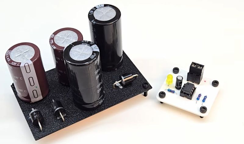
In the top photo on the left I see a power supply where I assumed 1/4inch wide tape would be all that’s needed. No conductive paint would work here for sure. I like the comment about negative space depth ‘traces” but at a DIP spacing that’s a mess.
I feel like a cricut could cut the traces from the tape then you could just slap them on some acrylic or perf or veroboard to get two sides.
Cool hack though I can see some modifications to this to make some cool stuff.
I made a Ender3 Mount for a cricut blade and wanted to cut holographic stickers. But with your idea might do this right after! Hope the blade wont dull too fast but I feel the blade in the blade holder is pretty standard even if the blade holder seems rather special.
That’s a really good idea. What are you using for your “build plate”?
Drag knife cutting copper is a thing, done for things like shielding. Your typical tape would be a bit thick for a CriCut, but you can get thinner, and the adhesive sheets tend to be thin.
Copper is a bit “gummy”, sharp blade & hold down well.
Kludgey but, hey, it’s an option to remember.
For such simple things it seems like dead bug soldering would be easier and just as effective. Of course sometimes things like this are more about trying to come up with a way with the materials on hand, and I understand that. Just a lot of work for a pretty suboptimal result anyway.
Conceptually interesting! There’s a couple tweaks that seem worth trying to me. Rather than emboss the trace, I would think it’d be easier to deboss it (cut it into the board) by just a little more than the thickness of the tape. That way, the traces would be protected from rubbing off. I’d also be interested in seeing what one could do with spray adhesive and aluminum foil in this configuration.
I think I’d still use proto/vector board just because this only really works with through hole components, but it’s good to have this trick in the mental toolbox, especially if one wanted a simple circuit directly integrated into their print.
I keep thinking: it’s a 3D printer. So you can make 3D shapes instead of 2D flat boards. I.e. you could print a circuit board in 3 dimensions and use this technique to integrate the circuit traces into the design. Like, merging industrial design with electronic design (the circuit IS the casing), or artful electronic display pieces.
This is actually a verry interesting idéa!
Hi Buckman, agreed!
In mid Jan 2026, I invented a process that leverages the ease of 3D printing to make rapid prototyping of multilayer PCBs attainable for those of us blessed to have 3D printers. After decades spent with protoboards, vero boards, and the like, it is nice to have a system that can give us rapid PCBs for our prototypes!
I just posted and open sourced my invention (with attribution) on substack:
https://open.substack.com/pub/josephmansour/p/open-source-diy-invention-rapid-pcb?r=2eqiyn&utm_campaign=post&utm_medium=web
Please consider joining my substack so you can contribute too :-)
I think the bit this concept works for if the DIY at home way to make circuit wrap around awkward project spaces – with the 3d printer concept like this you are not limited to planer circuit boards and interconnect wires, which on occasion at least could make this method very valuable.
As deadbug is cool to look at, might even be good enough for the electrical prototype but its also rather delicate so as a rule not well suited to actually becoming a functional prototype.
I have this tape, and the gum on the back makes for a dirty, soldering job, it burns and oozes out.
My off-the-wall hacky method is to powder coat the PCB with laser printer toner, and then selectively melt the toner with the laser engraver, then etch. So it’s like toner transfer, but laser printing directly on the PCB.
This sounds like a great idea! I wonder if it would work with regular black powder paint instead of toner. I suppose, as long as it absorbs the wavelength of your laser and sticks to the copper, any color would work.
I got a micro XY CNC that can cut grooves in a copper clad board. I have about $350 into it. And with a little extra setup you can swap the bit (manually) and have it drill out your holes too.
They sell a laser engraving attachment for it too, and maybe that would be interesting for a silk-screen like labeling on the copper? I wasn’t confident it would be worth the effort and extra step.
I wonder about using one of those new Vinyl cutting machines to cut the traces out?
Might work good.
Some ideas:
First google “plating plastic with copper” (eliminate the tape)
On the other side, you could also create component pockets in the 3D print, to give them better support.
You might also print a sort of solder stencil-like part that would press in and create a level looking surface after it was installed.
Might not be that practical (yet) but who knows where it may lead.
3D print solder paste? 🤔
Another comment suggested recessed traces to clean the rest by sanding, and with your suggestion that would work well
I like it sometimes you want a beautiful product without having to ship it off to a board manufacturer especially in the age of tariffs
Yes. Whatever are our opinions on the technicalities: it does look good. Beauty is in the eye of the beholder, and I think it could have been done a bit more artistically, given the amount of possibilities that the technique gives, but it does look good. :)
Just use conductive filament to make the traces. Then you can have as many trace layers in the board (ie: 3d object) as you want…
Is anyone here old enough to remember the days when pc boards were made with dry transfer film and resist tape?
It’s what this method reminded me of.
Yep. Never used it personally, but my dad did it professionally for prototyping purposes.
Or actually, probably he didn’t do full designs, but partial rework if a prototype had an issue.
I just buy 100pcs of these: https://hadex.cz/s006-cuprextit-50x60x15mm-cu35um-material-fr-4/
Costs roughly €10 for the whole bag. Then I cut copper tape as thin as required and simply apply it as needed. Then I solder the corners to make sure it’s connected. Since the board doesn’t flex and has a good ground plane on the other side, you get decent impedance control as a bonus.
When I need to connect MCU, e.g. RPi Pico, the easiest way is female header glued to the board lying on one side. Then run traces to the pins, bend them down as needed and solder them to the traces. It’s a good idea to run GND tape under the header and solder it to the ground plane. You can also trivially add SMA connectors. And since the board is rigid, you don’t have to worry when you fasten them.
I usually prep the board with 20P connector for a Pico project in 10 minutes tops. Then build the circuit on the board. I don’t use THT components at all, everything is SMD. I prefer 1206 capacitors and 0805 resistors, inductors. 0805 capacitors are too fragile. I have purchased rolls of 1000pcs resistors from 10Ω to 10MΩ in multiples of 10, plus some other values I tend to use, costs very little. Capacitors and inductors are more costly, but still manageable to buy in 50-200pcs quantities if you are a bit tactical about it.
For ICs, it’s obviously the larger the (leaded) package, the better. But when you flip it and secure with hot glue, even very low pitch parts are doable, it just costs a lot more time.
Lately I’ve been thinking about having boards with holes for the header and various IC pads premade. But the price deters me a bit.
I want to see a multilayer version! It might even be able to neatly recess the traces of the internal layer into the next layers backside!
Do the traces lowered instead. Then you can sand off the parts that shouldn’t conduct.
I don’t think that would sand nicely, I would rip and peel unpredictability
Depends on your tools. When everybody had a CNC mill, it was easier to etch the traces. Now everybody has a 3D printer, so……
I would think that the mill would be faster, though, and less fuss – using basically the same machine instructions, though subtractive, not additive.
I mean, “solution looking for a problem”…
I was experimenting with similar approaches few years back, I print pcb on Ende 3 but instead of extrude traces I did embossing – 0.5 mm then pushed copper foil in to it and after that sanded all that flat so only traces left. Is ok but for simple projects where you dont require small traces.
Hi Marcin, agreed!
In mid Jan 2026, I invented a comprehensive process that leverages the ease of 3D printing to make rapid prototyping of multilayer PCBs attainable for those of us blessed to have 3D printers. After decades spent with protoboards, vero boards, and the like, it is nice to have a system that can give us rapid PCBs for our prototypes!
I just posted and open sourced my invention (with attribution) on substack:
https://open.substack.com/pub/josephmansour/p/open-source-diy-invention-rapid-pcb?r=2eqiyn&utm_campaign=post&utm_medium=web
Please consider joining my substack so you can contribute too :-)
I guess the plastic melting around the heated pins is good to keep them in place, otherwise the thin copper foil would get pushed and ripped easily
Don’t want to be the complaining guy, but… why, really? When I was a kid I always wanted to have a CNC to make PCBs at home…
But nowadays nothing you could make yourself will get close to the $2 boards (with 4-layers!) you get from China. Yes, the shipping is slow, but is it a problem at all? If you have a full time job and this is a hobby, you can still work on the details and firmware on a breadboard while waiting for the first prototype. And then subsequent prototype iterations are even easier – just rework your previous prototype with kynar wire and move onto the clean next one when it arrives.
What if you printed the traces a little higher than that yet? And then you also printed a negative version.
Now it’s a stamp. Apply your copper tape. Squeeze it into the negative. Hopefully it cuts the copper at the edges of the traces and pushes the unwanted copper down into the valleys breaking contact with the traces.
Then just hope you can pull the pieces back apart! It might take some tweaking with ever-so slightly over-sizeing the traces on the negative so that you can pull it apart easily while still being tight enough to cut the copper tape.
Seems to me it would be easier to just use a Cricut to cut out the copper tape and apply it with transfer tape to the board.
I’m an EE and I have to say I think this is a great idea. 1. It lets you design the layout in CAD, which is easier than doing it on paper or manually transcribing from CAD. 2. The raised tracks make it easy to trace with a blade quick and clean. For 0.1in pitch designs it seems like a great method.
Most makers today have a 3D printer at the ready so it seems like a highly convenient option to me.
Hi Kman, agreed!
In mid Jan 2026, I invented a comprehensive process that leverages the ease of 3D printing to make rapid prototyping of multilayer PCBs attainable for those of us blessed to have 3D printers. After decades spent with protoboards, vero boards, and the like, it is nice to have a system that can give us rapid PCBs for our prototypes!
I just posted and open sourced my invention (with attribution) on substack:
https://open.substack.com/pub/josephmansour/p/open-source-diy-invention-rapid-pcb?r=2eqiyn&utm_campaign=post&utm_medium=web
Please consider joining my substack so you can contribute too :-)
IMao, what this is really missing is an automated process to cut the foil, doing that by hand isn’t great, I have tried it before and so have many others. There is a reason people have been looking for usable conductive printing materials. Have you tried inverting the circuit? Maybe then leather cutting tools could make this a bit more reasonable.
In the end it’s a useful technique so I don’t want to discount your efforts, but actual applicability is going to vary greatly.
Why not try hp copper filament and inlaying the copper.. would be able to just peel away the excess tape, and have the copper have some heat transfering property. Also by removing the poorly adhered top layer you could potentially just expose the copper traces :).. that’s what I would have tried =]
Hi Dan, agreed!
In mid Jan 2026, I invented a comprehensive process that leverages the ease of 3D printing to make rapid prototyping of multilayer PCBs attainable for those of us blessed to have 3D printers. After decades spent with protoboards, vero boards, and the like, it is nice to have a system that can give us rapid PCBs for our prototypes!
I just posted and open sourced my invention (with attribution) on substack:
https://open.substack.com/pub/josephmansour/p/open-source-diy-invention-rapid-pcb?r=2eqiyn&utm_campaign=post&utm_medium=web
Please consider joining my substack so you can contribute too :-)
I thought of something similar when I bought my first 3d printer back 2016. It quickly evolved into making the “traces” trenches I cut lay wire into instead of tape and using a wire wrap tool. But once you reach that point, you might as well by nonconductive perf board and either solder or wire wrap.
Has nobody commented on the implications that any kind of heat will melt this plastic and turn the project into unusable goo?
Print in anything but the really low temp softening PLA family and it will be very little if any different in practice to the FR4 board based circuit in regard to temperature failure, even if the method of failure is different as the vast majority will be component failure through overheating long before substrate notices.
Hi Foldi-One, bingo there are many resins/filament types that can handle higher temperatures just fine.
In mid Jan 2026, I invented a comprehensive process that leverages the ease of 3D printing to make rapid prototyping of multilayer PCBs attainable for those of us blessed to have 3D printers. After decades spent with protoboards, vero boards, and the like, it is nice to have a system that can give us rapid PCBs for our prototypes!
I just posted and open sourced my invention (with attribution) on substack:
https://open.substack.com/pub/josephmansour/p/open-source-diy-invention-rapid-pcb?r=2eqiyn&utm_campaign=post&utm_medium=web
Please consider joining my substack so you can contribute too :-)
I already tried using copper tape to build small pads to solder Manhattan style, the adhesive doesn’t stand the solder heat and they detach easily. It can work with a large ground screen with one solder joint, but slim traces or small pads are different things.