 In a recent video [QWZ Labs] demonstrates an interesting technique to use 3D printing to make creating custom PCBs rather straightforward even if all you have is a 3D printer and a roll of copper tape.
The PCB itself is designed as usual in KiCad or equivalent EDA program, after which it is exported as a 3D model. This model is then loaded into a CAD program – here Autodesk Fusion – which is used to extrude the traces by 0.6 mm before passing the resulting model to the 3D printer’s slicer.
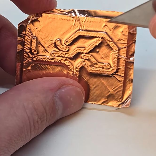
By extruding the traces, you can subsequently put copper tape onto the printed PCB and use a cutting tool of your choice to trace these raised lines. After removing the rest of the copper foil, you are left with copper traces that you can poke holes in for the components and subsequently solder onto.
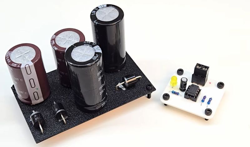
As far as compromises go, these are obviously single-sided boards, but you could probably extend this technique to make double-sided ones if you’re feeling adventurous. In the EDA you want to use fairly thick, 2 mm trace width with plenty of clearance to make your copper cutting easy, while in the slicer you have to check that the traces get printed properly. Using the Arachne wall generator option for example helps to fill in unpleasant voids, and the through-holes ought to be about 1 mm at least lest the slicer decides that you really want to drill them out later by hand instead.
While soldering is pretty easy on copper tape like this, desoldering would be more challenging, especially with hot air. In the video PLA was used for the PCB, which of course is rather flexible and both softens and melts easily when exposed to heat, neither of which make it look very good compared to FR4 or even FR1 PCB materials. Of course, you are free to experiment with whatever FDM, SLA or even SLS materials you fancy that would work better for the board in question.
Although obviously not a one-size-fits-all solution for custom PCBs, it definitely looks a lot easier than suffering through the much-maligned prototype perfboards that do not fit half the components and make routing traces hell. Now all we need is the ability to use e.g. targeted vapor-deposition of copper to make fully 3D printed PCBs and this method becomes even easier.


Kinda…silly!
If you’re making circuit boards that simple, use MDF or something and paste strips of copper tape on it.
Or better draw your circuit on a copper clad board with a permanent marker, and then etch it. Don’t even need to open kicad
Pretty sure its a proof of concept. 🙄
This ^^^^ takes less time, can use toner transfer also.
If all you have is a hammer, everything g looks like a nail.
But joking aside – nice idea but rather pointless. If you cut the traces by hand anyway, you could as well start from a print on paper.
But can this be extended? You still print the traces as extruded and raised paths. Then you flip the part and dip it into… conductive ink? Just enough to cover tr traces, but leaving the gaps. Or maybe use a paint roller with conducive paint? Or maybe roll on some glueand attach a conductive foil? But you would need a way to trim the excess easily (maybe with a brush like in gold plating?)
Invert the process. Sink the traces into the substrates and cover with copper foil, then compress the board against a soft anvil, like a rubber pad, which pushes the traces into the grooves. Now the parts that you’re supposed to remove are raised and can be sanded off all at once.
When I saw the foil over the raised plastic picture I thought is he going to put glue on the raised portion and stick it to something and peal the rest off?
You could speed up the process a lot by making the print negative (traces indented), sticking on the copper tape, press it down good in all nooks and crannies, and then sanding the copper down to the plastic. As the traces that you want are indented, that’s what you’re left with. Sanding is a lot faster than tracing the traces with a knife. Not to mention a lot less fiddly, as you won’t accidentally pull the copper trace off the ridge, like in this video.
I feel like a cricut could cut the traces from the tape then you could just slap them on some acrylic or perf or veroboard to get two sides.
Cool hack though I can see some modifications to this to make some cool stuff.
Kludgey but, hey, it’s an option to remember.
For such simple things it seems like dead bug soldering would be easier and just as effective. Of course sometimes things like this are more about trying to come up with a way with the materials on hand, and I understand that. Just a lot of work for a pretty suboptimal result anyway.
I have this tape, and the gum on the back makes for a dirty, soldering job, it burns and oozes out.
My off-the-wall hacky method is to powder coat the PCB with laser printer toner, and then selectively melt the toner with the laser engraver, then etch. So it’s like toner transfer, but laser printing directly on the PCB.
I got a micro XY CNC that can cut grooves in a copper clad board. I have about $350 into it. And with a little extra setup you can swap the bit (manually) and have it drill out your holes too.
They sell a laser engraving attachment for it too, and maybe that would be interesting for a silk-screen like labeling on the copper? I wasn’t confident it would be worth the effort and extra step.
I wonder about using one of those new Vinyl cutting machines to cut the traces out?
Might work good.