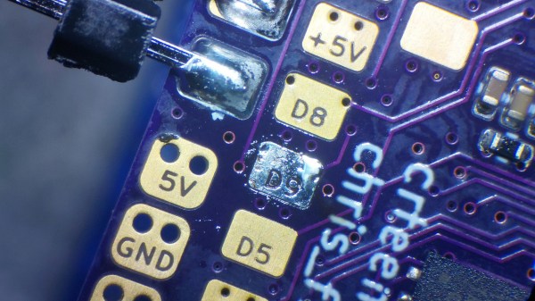
When making a PCB informative and self-documenting, there’s often just not enough space to silkscreen all the labels you want, and slowly but surely, you collect a set of tricks: using different through-hole pad shapes to denote ground or power pins, standardized pinouts for connectors, your own signal name shortening notations, and so on.
What if you have some large-ish signal pads on your board, and having the signal names on silkscreen just isn’t good enough? In this case, here’s a new trick for your toolkit: [Christoph] from [MakerProbe] shows us how he puts text directly inside the copper pads.
What you need is a set of Gerber files and a Python script. Technically, this ought to work with any PCB EDA, with [Christoph] using KiCad. You need to put the to-be-subtracted signal names on their very own layer, export Gerber files without features like aperture macros, then run the script. You’ll get a new copper layer as a result, it’s that simple. We also get a set of tips on what kinds of pads suit best and how to prepare them — and fancy-looking real-life examples. You get higher resolution than for on-silkscreen text, solderability isn’t impacted, and the labels are even visible after desoldering wires from the pads. What’s not to like?
Over on Twitter, [Makerprobe] have been doing things like 0201 tombstoning and BGA yield research – we say they’re worth a follow if you’d like to see someone pushing PCB boundaries! Innovative PCB design methods and tricks have a special spot in our hearts, what’s with things like this Tux-emblazoned desktop motherboard that’s also a guide on PCB aesthetics, and there’s a whole lot more you can do to make your PCBs pretty while preserving and even improving functionality. From turning rigid PCBs flexible to hiding components inside a PCB stack, there’s plenty of opportunities that we are yet to extract out of PCB world, and it’s lovely to see one more technique we can make use of.


