V-Cut Vias Test Your Whole Panel At Once

We might consider PCB panels as simply an intermediate step towards getting your PCBs manufactured on the scale of hundreds. This is due to, typically, an inability to run traces beyond your board – and most panel generators don’t give you the option, either. However, if you go for hand-crafted panels or modify a KiKit-created panel, you can easily add extra elements – for instance, why not add vias in the V-Cut path to preserve electrical connectivity between your boards?

[Adam Gulyas] went out and tried just that, and it’s a wonderfully viable method. He shows us how to calculate the via size to be just right given V-Cut and drilling tolerances, and then demonstrates design of an example board with discrete component LED blinkers you can power off a coin cell. The panel gets sent off to be manufactured and assembled, but don’t break the boards apart just yet — connect power to the two through-hole testpoints on the frame, and watch your panel light up all at once.

It’s a flashy demonstration – even more so once you put light-diffusing spheres on top of the domes. You could always do such a trick with mousebites, but you risk having the tracks tear off the board, and, V-Cuts are no doubt the cleanest way to panelize – no edge cleaning is required after breaking the boards apart. Want to learn about panel design? We’ve written and featured multiple guides for you over the years.

Need High-Power Li-Ion Charging? How About 100 W

Ever want a seriously powerful PCB for charging a Li-Ion pack? Whatever you want it for, [Redherring32] has got it — it’s a board bearing the TPS25750D and BQ25713 chips, that lets you push up to 100 W into your 1S Li-Ion pack through the magic of USB Power Delivery (USB-PD).

Why do you need so much power? Well, when you put together a large amount of Li-Ion cells, this is how you charge it all at once – an average laptop might charge the internal battery at 30 W, and it’s not uncommon for laptop batteries to be dwarfed by hackers’-built packs.

A 4-layer creation peppered with vias, this board’s a hefty one — it’s not often that you see a Li-Ion charger designed to push as much current as possible into a cell, and the chips are smart enough for that. As far as the onboard chips’ capabilities go, the board could handle pack configurations from 1S to 4S, and even act as a USB-PD source — check the IC configuration before you expect to use it for any specific purpose.

Want a simpler charger, even if it’s less powerful? Remember, you can use PPS-capable PD chargers for topping up Li-Ion packs, with barely any extra hardware required.

3D Print A Stenciling Frame For Your PCB

For many a hacker, stenciling a board for the first time is a game-changing experience – the solder joints you get, sure do give your PCB the aura of a mass-manufactured device. Now, you might not get a perfect print – and neither did [Atul R]. Not to worry, because if you have a 3D printer handy, he’s showing you how to design a 3D-printed frame using Blender and TinkerCAD, making your solder paste print well even if you’re trying to rest a giant stencil on top of a tiny board.

[Atul]’s situation was non-characteristic – the project is a 2mm thick PCB designed to plug right into a USB port, so the usual trick of using some scrap PCBs wouldn’t work, and using a 3D-printed frame turned out to be key. To get it done, he exported a .wrl from KiCad, processed it in Blender, and then designed a frame with help of TinkerCAD. These techniques, no doubt, will translate into your CAD of choice – especially if you go with .step export instead of .wrl.

This kind of frame design will get you far, especially for boards where the more common techniques fail – say, if you need to assemble a double-sided board and one side is already populated. Don’t have a stencil? You could surely make a 3D printed stencil, too, both for KiCad boards and for random Gerber files. Oh, and don’t forget this 3D-printable stencil alignment jig, while you’re at it – looks like it ought to save you quite a bit of trouble.

Pi Zero Power Optimization Leaves No Stone Unturned

If you’ve ever designed a battery-powered device with a Pi Zero, you have no doubt looked into decreasing its power consumption. Generic advice, like disabling the HDMI interface and the onboard LED, is omnipresent, but [Manawyrm] from [Kittenlabs] goes beyond the surface-level, and gifts us an extensive write-up where every recommendation is backed with measurements. Armed with the Nordic Power Profiler kit and an SD card mux for quick experimentation, she aimed at two factors, boot time and power consumed while booting, and made sure to get all the debug information we could use.

Thanks to fast experimentation cycles and immediate feedback, we learn plenty of new things about what a Pi Zero does and when, and how we can tame various power-hungry aspects of its behavior. Disabling the GPU or its aspects like HDMI output, tweaking features like HAT and other peripheral probing, and even tactical overclocking during boot – it’s an extensive look at what makes a Pi Zero tick, and no chance for spreading baseless advice or myths.

All in all, this write-up helps you decrease the boot time from twelve seconds to just three seconds, and slash the power budget of the boot process by 80%. Some recommendations are as simple as config.txt entries, while others require you to recompile the kernel. No matter the amount of effort you can put into power optimization, you’ll certainly find things worth learning while following along, and [Manawyrm]’s effort in building her solar-powered Pi setup will help us all build better Pi-Zero-powered solar devices and handhelds.

Laptop GPU Upgrade With Just A Little Reballing

Modern gaming laptops are in an uncomfortable spot – often too underpowered for newest titles, but too bulky to be genuinely portable. It doesn’t help they’re not often upgradeable, so you’re stuck with what you’ve bought – unless, say, you’re a hacker equipped some tools for PCB reflow? If that’s the case, welcome to [TechModLab]’s video showing you the process of upgrading a laptop’s soldered-on NVIDIA GPU, replacing the 3070 chip with a 3080.

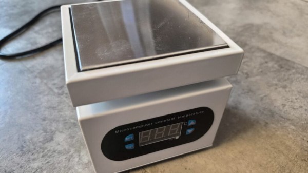
You don’t need much – the most exotic tool is a BGA rework station, holding the mainboard steady&stiff and heating a specific large chip on the board with an infrared lamp from above. This one is definitely a specialty tool, but we’ve seen hackers build their own. From there, some general soldering tools like flux and solder wick, a stencil for your chip, BGA balls, and a $20 USB-C hotplate are instrumental for reballing chips – tools you ought to have.

Reballing was perhaps the hardest step of the journey – instrumental for preparing the GPU before the transplant. Afterwards, only a few steps were needed – poking a BGA ball that didn’t connect, changing board straps to adjust for the new VRAM our enterprising hacker added alongside the upgrade, and playing with the driver process install a little. Use this method to upgrade from a lower-end binned GPU you’re stuck with, or perhaps to repair your laptop if artifacts start appearing – it’s a worthwhile reminder about methods that laptop repair shops use on the daily.

Itching to learn more about BGAs? You absolutely should read this article series by our own [Robin Kearey]. We’ve mostly seen reballing used for upgrading RAM on laptop and Raspberry Pi boards, but seeing it being used for an entire laptop is nice – it’s the same technique, just scaled up, and you always can start by practicing at a smaller scale. Now, it might feel like we’ve left the era of upgradable GPUs on laptops, and today’s project might not necessarily help your worries – but the Framework 16 definitely bucks the trend.

Continue reading “Laptop GPU Upgrade With Just A Little Reballing”

MikroPhone – Open, Secure, Simple Smartphone

Modern smartphones try and provide a number of useful features to their users, and yet, they’re not exactly designed with human needs in mind. A store-bought smartphone will force a number of paradigms and features onto you no matter whether you want them, and, to top it off, it will encroach on your privacy and sell your data. It’s why self-built and hacker-friendly smartphone projects keep popping up, and the MikroPhone project fills a new niche for sure, with its LTE connectivity making it a promising option for all hackers frustrated with the utter state of smartphones today.

MikroPhone is open-source in every single aspect possible, and it’s designed to be privacy-friendly and easy to understand. At its core is a SiFive Freedom E310, a powerful RISC-V microcontroller – allowing for a feature phone-like OS that is easy to audit and hard to get bogged down by. You’re not limited to a feature phone OS, however – on the PCB, you will find a slot for an NXP i.MX8M-based module that can run a Linux-based mobile OS of your choice. MikroPhone’s display and touchscreen are shared between the Linux module and the onboard MCU, a trick that reminds us of the MCH2022 badge – you get as much “smartphone” as you currently need, no more, no less.

The cool features at MikroPhone’s core don’t end here. The MikroPhone has support for end-to-end encrypted communications, kept to its feature-phone layer, making for a high bar of privacy protection – even when the higher-power module might run an OS that you don’t necessarily fully trust. Currently, MikroPhone is a development platform, resembling the PinePhone’s Project Don’t Be Evil board back when PinePhone was just starting out, and just like with PinePhone, it wouldn’t be hard to minify this platform into a pocket-friendly form-factor, either. The PinePhone has famously become a decent smartphone replacement option in the hacker world, even helping kick off a few mobile OS projects and resulting in a trove of hacks to grace our pages.

Easily Build This IMU Array Sandbox

These days we’re used to our devices containing an inertial measurement unit (IMU) that lets it know its position relative to the Earth. They’re mechanical devices at heart, and so they’re not infallible, with a few well-known failure modes — but we can try and help it. One way that’s getting some attention is to put many MEMS IMUs on a single PCB, connect it to an FPGA, then process their data all together to make for a more sensitive IMU or filter out drift. Want to join in? Here’s an open source implementation from [will127534].

With 32 individual ICM-42688-P SPI-connected IMUs and the beloved ICE40 chip at the center of the board, this PCB is a powerful platform to help you jump onto the new direction of the IMU research world. There’s example Verilog code that tests the board’s workings, and you can pair it with a Pi Pico running MicroPython to test out its raw capabilities. After that, the stage is yours.

The board is cheap to order online, easy to assemble yourself if you must, or have JLCPCB assemble it — just solder some capacitors on the backside afterwards. There’s a breakout, but it’s mostly for tests. This board is very much designed to be a module in a bigger system, [will] mentions that he’s building a geophone. Clever array-based hacks are en vogue, it would feel – here’s a LED array from [mitxela] that uses LEDs as sensors.