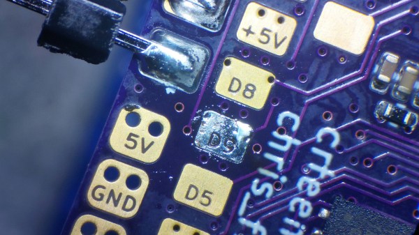
One of the extra tools someone might need when working with surface-mount components is a solder paste stencil, which not only simplifies the application of solder paste to a PCB but increases accuracy. These metal stencils can cost an annoying amount of money and take time to get delivered, so this group has developed a method to 3D print them instead.
Starting with a PCB design in one’s tool of choice, the Gerber files can be sent to the online Stenchill tool to generate the stencil. Alternatively, a KiCad plugin exists as well. The tool will output files for a 3D printer from there. An FDM printer is required, with either PLA or PETG filament, and some configuration in the slicer is needed to get the accuracy required for a useful stencil. But once that’s all set up, the printer can output a perfectly usable stencil at a fraction of the cost, and without having to wait days for delivery through the mail.
It’s not all upside, though. Although it might be better than applying solder paste with a syringe on a massive board or doing more than one smaller board by hand, it may not be as good as a metal stencil for extremely small pads. But for those who often find themselves using metal stencils and dealing with the downsides that come with them, this could be a viable alternative, especially when prototyping.
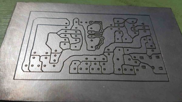
If you have a laser cutter handy, that opens up some additional options for stencil production.
Continue reading “Saving Some Coin With 3D Printed Stencils”