By now, we’ve gone through LiIon handling basics and mechanics. When it comes to designing your circuit around a LiIon battery, I believe you could benefit from a cookbook with direct suggestions, too. Here, I’d like to give you a collection of LiIon recipes that worked well for me over the years.
I will be talking about single-series (1sXp) cell configurations, for a simple reason – multiple-series configurations are not something I consider myself as having worked extensively with. The single-series configurations alone will result in a fairly extensive writeup, but for those savvy in LiIon handling, I invite you to share your tips, tricks and observations in the comment section – last time, we had a fair few interesting points brought up!
The Friendly Neighborhood Charger
There’s a whole bunch of ways to charge the cells you’ve just added to your device – a wide variety of charger ICs and other solutions are at your disposal. I’d like to focus on one specific module that I believe it’s important you know more about.
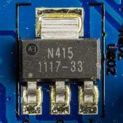
You likely have seen the blue TP4056 boards around – they’re cheap and you’re one Aliexpress order away from owning a bunch, with a dozen boards going for only a few bucks. The TP4056 is a LiIon charger IC able to top up your cells at rate of up to 1 A. Many TP4056 boards have a protection circuit built in, which means that such a board can protect your LiIon cell from the external world, too. This board itself can be treated as a module; for over half a decade now, the PCB footprint has stayed the same, to the point where you can add a TP4056 board footprint onto your own PCBs if you need LiIon charging and protection. I do that a lot – it’s way easier, and even cheaper, than soldering the TP4056 and all its support components. Here’s a KiCad footprint if you’d like to do that too.
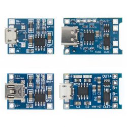 This is a linear charger IC – if you want 1 A out, you need 1 A in, and the input-output voltage difference multiplied by current is converted into heat. Thankfully, the TP4056 modules are built to handle high temperatures reasonably well, and you can add a heatsink if you want. Maximum charging current is set by a resistor between ground and one of the pins, default resistor being 1.2 kΩ resulting in 1 A current; for low-capacity cells, you can replace it with a 10 kΩ resistor to set a 130 mA limit, and you can find tables online for intermediate values.
There’s some cool things about the TP4056 IC that most people don’t know about if they’re using the modules as-is. The IC’s CE pin is hardwired to 5 V VIN, but if you lift that pin, you can use it to disable and enable charging with a logic level input from your MCU. You can monitor the charging current by connecting your MCU’s ADC to the PROG pin – the same pin used for the current setting resistor. There’s also a thermistor pin, typically wired to ground, but adaptable for a wide range of thermistors using a resistor divider, whether it’s the thermistor attached to your pouch cell or one you added externally to your 18650 holder.
 There’s problems with the TP4056 too – it’s a fairly simple IC. Efficiency isn’t an imperative where wall power is available, but the TP4056 does waste a decent bit of power as heat. A switching charger-based module avoids that, and often also lets you charge at higher currents if ever required. Connecting a cell in reverse kills the chip, and the protection circuit too – this mistake is easy to make, I’ve done that aplenty, and this is why you need spares. If you reverse the cell contacts, throw the board out – don’t charge your cells with a faulty IC.
Also, given the TP4056’s popularity, copies of this IC are manufactured by multiple different chip vendors in China, and I’ve observed that some of these copy ICs break more easily than others, for instance, no longer charging your cells – again, keep spares. The TP4056 also doesn’t provide charging timers like other, more modern ICs do – a subject we touched upon in the comment section of the first article.
All in all, these modules are powerful and fairly universal. It’s even safe to use them to charge 4.3 V cells, as due to the CC/CV operation, the cell simply won’t charge to its full capacity – prolonging your cell’s life as a side effect. When you need to go beyond such modules, there’s a myriad of ICs you can make use of – smaller linear chargers, switching chargers, chargers with built-in powerpath and/or DC-DC regulator features, and a trove of ICs that do LiIon charging as a side effect. The world of LiIon charger ICs is huge and there’s way more to it than the TP4056, but the TP4056 is a wonderful starting point.
The Protection Circuit You Will See Everywhere
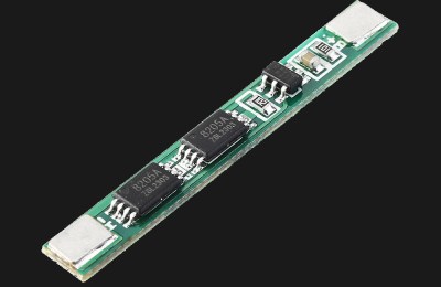
Just like with charging ICs, there’s many designs out there, and there’s one you should know about – the DW01 and 8205A combination. It’s so ubiquitous that at least one of your store-bought devices likely contains it, and the TP4056 modules come with this combo too. The DW01 is an IC that monitors the voltage of your cell and the current going to and from it, and the 8205A is two N-FETs in a single package, helping with the actual “connect-disconnect the battery” part. There’s no additional current sensing resistor – instead, the DW01 monitors voltage across the 8205A junction. In other words, the same FETs used to cut the cell from the outside world in case of failure, are used as current sensing resistors. This design is cheap, prevalent, and works wonders.
 The DW01 protects from overcurrent, overdischarge and overcharge – the first two happen relatively often in hobby projects, and that last one’s handy if your charger ever goes rogue. If something wrong happens, it interrupts the connection between the cell’s negative terminal and GND of your circuit, in other words, it does low-side switching – for a simple reason, FETs that interrupt GND are cheaper and have lower resistance. We’ve also seen some hacks done with this chip – for instance, we’ve covered research from a hacker who figured out that the DW01 can be used as a soft power switch for your circuit – in a way that doesn’t compromise on safety. You only need to connect a GPIO pin of your MCU to the DW01, preferably through a diode – this comment describes an approach that seems pretty failure-resistant to me.
When you first connect a LiIon cell to the DW01+8205A combination, sometimes it will enable its output, but sometimes it won’t. For instance, if you have a holder for 18650s and a protection circuit connected to it, it’s a 50/50 chance that your circuit will power up once you insert the battery. The solution is simple – either connect a charger externally, or short-circuit the OUT- and B- with something metal (I often add an external button), but it’s annoying to deal with. Just like TP4056, the DW01+8205A combo dies if you connect the battery in reverse. Also, the DW01 is internally wired for 2.5 V overdischarge cutoff, which technically isn’t changeable. If you don’t have a separate software-controlled cutoff, the FS312 is a pin-compatible DW01 replacement with 3.0 V overdischarge point, helping you prolong your cell’s life.
You can buy a batch of ready-to-go protection circuit modules, or just use the protection circuit laid out on the TP4056 module PCB. You can also accumulate a decent stock of protection circuits by taking them out of single-cell batteries whenever the cell puffs up or dies – take caution not to puncture the cell while you do it, please.
All The Ways To Get 3.3 V
For a 4.2 V LiIon cell, the useful voltage range is 4.1 V to 3.0 V – a cell at 4.2 V quickly drops to 4.1 V when you draw power from it, and at 3.0 V or lower, the cell’s internal resistance typically rises quickly enough that you will no longer get much useful current out of your cell. If you want to get to 1.8 V or 2.5 V, that is not a problem, and if you want to get to 5 V, you’ll use a boost regulator of some sort. However, most of our chips still run at 3.3 V – let’s see what our options are here.
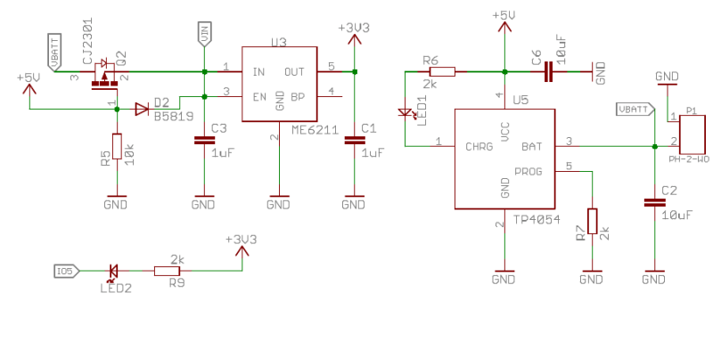
When it comes to LiIon range to 3.3 V regulation, linear regulators closely trail switching regulators in terms of efficiency, often have lower quiescent (no-load) current if you seek low-power operation, and lower noise if you want to do analog stuff. That said, your regular 1117 won’t do – it’s an old and inefficient design, and the 1117-33 starts grinding its gears at about 4.1 V. Instead, use pin-compatible, low dropout voltage replacements like AP2111, AP2114 and BL9110, or AP2112, MIC5219, MCP1700 and ME6211 if you’re okay with SOT23 stuff. All of these are linear regulators comfortable providing 3.3 V with input down to 3.5 V and sometimes even 3.4 V, if you’d like to power something like an ESP32. It’s hard to deny the simplicity of using a linear regulator – one chip and a few caps is all it takes.
If you want 500 mA to 1000mA or even more current on an ongoing basis, a switching regulator will be your best friend. My personal favourite is PAM2306 – this regulator is used on the Raspberry Pi Zero, it’s very cheap and accessible, and even has two separate output rails. Given its capability to do 100% duty cycle operation, it can extract a lot of juice out of your cells, often desirable for higher-power projects where runtime matters. And hey, if you got Pi Zero with a dead CPU, you won’t go wrong snipping a part of the PCB off and soldering some wires to it. When designing your own board, use datasheet recommendations for inductor parameters if the whole “picking the right inductor” business has you confused.
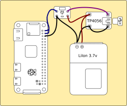 So, the PAM2306 is the regulator on the Pi Zero, and it’s also LiIon-friendly? Yep, you can power a Pi Zero directly from a LiIon battery, as all the onboard circuitry works down to 3.3 V on the “5 V” pins. I’ve tested it extensively in my own devices, and it even works with the Pi Zero 2 W. Combined with this powerpath and a charger, you have a complete “battery-powered Linux” package, with all the oomph that a Raspberry Pi provides – at cost of only a handful of components. One problem to watch out for is that MicroUSB port VBUS will have battery voltage – in other words, you’re best off filling the MicroUSB ports with hot glue just in case someone plugs a MicroUSB PSU there, and tapping the USB data testpoints for USB connectivity.
A Power Path To Join Them All
Now, you’ve got charging, and you got your 3.3 V. There’s one problem that I ought to remind you about – while you’re charging the battery, you can’t draw current from it, as the charger relies on current measurements to control charging; if you confuse the charger with an extra load, you risk overcharging the battery.
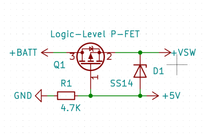
Fortunately, since you have a charger plugged in, you must have 5 V accessible. It’d be cool if you could power your devices from that 5 V source when it’s present, and use the battery when it’s not! We typically use diodes for such power decisions, but that’d cause extra voltage drop and power losses when operating from the battery. Thankfully, there’s a simple three-component circuit that works way better.
In this power path circuit, a P-FET takes role of one of the diodes, with a resistor opening the FET while the charger’s not present. The P-FET doesn’t have a voltage drop, but instead has resistance in fractions of an ohm, so you avoid losses when the charger’s not plugged in. Once the charger is connected, the FET closes, and the charger powers your circuit through the diode instead. You need a logic-level P-FET – IRLML6401, CJ2305, DMG2301LK or HX2301A would fit, and there’s thousand others that will work. As for a diode, a default Schottky like 1N5819 (SS14 for SMD) will do. It’s a ubiquitous circuit and deserves its place in circuit toolboxes.
You can buy shields and modules that contain all of these parts and sometimes more, on a single board. You can also buy ICs that contain all or some of the parts of this circuit, often improved upon, and not worry about the specifics. These ICs tend to be more expensive, however, and way more subject to chip shortages than the individual component-based solution. Plus, when issues arise, understanding of inner workings helps a whole lot. Thus, it’s important that the basics are demystified for you, and you don’t feel forced into reusing powerbank boards next time you want to make a device of yours portable.
Be on the lookout on what other boards are doing. Often, you’ll see the charger + regulator + powerpath circuit described above, especially when it comes to cheaper boards with chips like the ESP32. Other times, you’ll see more involved power management solutions, like powerbank chips or PMICs. Sometimes they’re going to work way better than the simple circuit, sometimes it’s the opposite. For instance, some TTGO battery-powered boards use powerbank chips and overcomplicate the circuit, resulting in weird behaviour and malfunctions. A different TTGO board, on the other hand, uses a PMIC that’s way more suited for such boards, which results in flawless operation and even granular power management control for the user.
Hack Portable Devices Like You Couldn’t Before
Now you know what it takes to add a LiIon battery input connector to your project, and the secrets behind the boards that come with one already. It’s a feeling like no other, taking a microcontroller project with you on a walk as you test out a concept of yours. I hope I got you a bit closer to experiencing it.
Next time, I’d like to talk about batteries with multiple cells in series – BMSes, balancing and charging LiIon packs from different sources. That, however, will take a good amount of time for me to prepare, as I’d like to finish a few related projects first, and I recommend you check this coverage of ours out if you’d like to learn about that. In the meantime, I wish you luck in building your battery-powered projects!


“while you’re charging the battery, you can’t draw current from it, as the charger relies on current measurements to control charging; if you confuse the charger with an extra load, you risk overcharging the battery”
I was pointed at another website recently that said something similar… and I have to hard disagree. A charger is already in constant-voltage mode when nearing the termination point. It’s simply *not possible* to overcharge in this part of the regime, as the charge current asymptotically approaches zero as the cell voltage approaches the charge voltage and is therefore self-limiting. The 0.1C charge termination feature is just an efficiency measure, as the charger otherwise wastes power being enabled unnecessarily when the cell is fully charged – but if it is prevented from activating because an additional load is drawing current, you don’t want to disable the charger anyway, because it’s powering the load instead!
Yeah – it is likely you won’t be able to get the battery charged to 100% full when drawing a load current simultaneously, but I don’t see how it could cause overcharging or other dangers.
Only if the charger has some sort of “gas gauge” circuitry that counts coulombs going into the battery and tries to estimate its state of health of something.
And if the charger is that smart, it’s also guaranteed to have an explicit connection for the load, so that the gas gauge can actually do it’s job properly.
Your page spreads positivity that empowers readers to pursue goals confidently, and I hope you can also check my website to discover more inspiring content designed to encourage progress.
skip bins
Guess you mean this site: https://www.best-microcontroller-projects.com/tp4056.html
I stumbled across it recently, too and was wondering.
Haven’t had any problems with those boards yet, though…
I’ve often been scared off by the “Woo wooooo, drawing power and charging is bad medicine, boogedy boogedy.” but had not been able to dig up clear justification for it.
“The 0.1C charge termination feature is just an efficiency measure” umm, actually no. Unlike lead-acid and maybe other chemistries, a constant trickle charge will significantly shorten the life of a lithium battery. I don’t remember the details, but I think it has to do with the lithium being electroplated onto somewhere it doesn’t belong.
You probably shouldn’t “um, actually” unless you *actually* know. And this isn’t really trickle charging – that implies always pushing current into the cell, but here we’re purely talking about when a load is active. When the load is switched off, the charger will terminate again.
Now, it’s *absolutely* possible to be kinder to a cell by actively controlling when the charger is enabled to give it some hysteresis, but the original claim was that the pasive configuration would risk dangerously overcharging the cell, which is categorically false.
You cannot “trickle charge” a lithium battery. If you keep pushing current in, the voltage just keeps on rising until the battery catches fire. If you keep a constant voltage, the current eventually becomes zero. The voltage efficiency of a a lithium cell is something like 99.98% – it doesn’t have any meaningful hysteresis in charging except for what happens with the internal resistance.
Trickle charging is only possible with batteries which require a significant “over-potential” to charge, such as lead acid batteries that need extra voltage before the chemical reaction actually takes place. When you keep the battery at that threshold, it is constantly passing some current through without actually charging the cells. Hence why the voltage of a full 12 Volt battery is 14.4 Volts when charging and 13.2 Volts when resting. This is actually a useful feature, because series connected cells stop charging before they stop passing current, which equalizes the battery when you top it up.
“When you first connect a LiIon cell to the DW01+8205A combination, sometimes it will enable its output, but sometimes it won’t. For instance, if you have a holder for 18650s and a protection circuit connected to it, it’s a 50/50 chance that your circuit will power up once you insert the battery. The solution is simple – either connect a charger externally, or short-circuit the OUT- and B- with something metal (I often add an external button), but it’s annoying to deal with. ”
WHAT THE!!! I bought 10 LiPo protection boards which specifically disconnect at 3V, not 2.4 or less. But I never got those working e.g. get voltage out the B+/B-. I googled my arse off, checked circuit…
And now this worked. THANK YOU!
Helluva “gotcha,” ain’t it? ;-)
That one got me about 10 years ago, too. I was (re-)building a Li-Ion pack for a netbook, with an unfamiliar controller IC on its PCB. After soldering everything up — yes, the cells had solder eyelets tack-welded onto the ends of each 18650 — it was completely dead, as far as the netbook charging circuit was concerned. I spent days trying to figure out what had gone wrong. Everything I checked with my multimeter indicated that it *should* be working fine, yet there was no voltage at the power connector pins.
IIRC, it was a few weeks later that, by pure accident I assure you, I shorted the two negative nodes (probably to temporarily bypass the MOSFETs), and suddenly it came back to life.
Wouldn’t the 4.7k resistor between the 5V and the ground consume more than a simple diode would consume ?
nope, it’s only a 1mA => 0.005W load, compared to the 5W peak TP4056 + whatever your SBC would consume from the 5V rail, it’s nothing!
And there’s really no reason to have it only 4.7k, it could easily be 100k. But it’s a non-issue anyway, because it only draws power when +5V is connected. If simply using diodes, that requires a diode on the battery line and therefore causes a voltage drop when running off the battery.
I’ve experienced brownouts on charger disconnect when the resistor was 10K (Pi Zero + TP4056 set to 1A), that were solved by decreasing the resistor value. The lower the resistor value, the less time it takes for the FET to open – and given all the capacitors typically present on the 5V input plus my anecdotal experience, I’d wager lower values are indeed helpful in preventing brownouts as the 5V charger is unplugged. The internal diode should theoretically prevent the “brownout when FET not open” failure mode, but I’d guess it’s only good for so much.
The internal diode is basically a parasitic structure and typically has a quite high forward voltage and bad switching capability (slow turnoff). One may add a second SS14 or use a FET with an extra diode built-in, or add the high-value resistor in series with the 4k7 and bridge it with a push button before disconnecting (sacrificing some of the circuits simplicity)
1 mA is a bit too much for battery powered applications, still, especially if it’s always present.
but it’s not always present – that 1mA is only consumed when the charger is plugged in!
If that resistor is just to keep the gate near ground, you may go way up with the value. The voltage drop across the resistor at the leakage current of the diode has to be smaller than the threshold voltage of the FET (assuming the leakage into the gate may be neglected).
There is a gate charge characteristic in the MOSFET, and that must be discharged through the resistor. The larger the resistance, the slower the MOSFET will turn off. That’s fine for a lot of applications, but may lead to slower than you want voltage rail ramping that may lead to undefined behavior of your ICs. Maybe with a proper powergood signal you can get around that.
Maybe there’s an obvious solution to this, but what I’m missing is one of those charging circuits that also break out the USB data lines. What if I wanted to use the USB port on my portable device for both charging a LiPo battery and/or serial communication with a 5V powered device? Is it OK to bring the data lines past my 3.7 -> 5V boost converter and into my microcontroller (or say, a USB sound card)?
In my experience, you can just pass the data signals through. Provided they also share a ground. Both devices can be powered separately
1A TP4056 chargers might damage normal USB ports. They don’t verify that the port is capable of providing 1A without catching fire before they try to draw that much. To be exact they should check if the port can provide that much current and the cable is capable of carrying that much current.
I went down the rabbit hole this weekend and gathered information about the USB fast charging protocols out there:
On USB 1.1 ports a device may draw 100mA, on USB 2.0 ports 500mA and on USB 3.0 ports 900mA as specified in the configuration descriptor accepted by the host. In unconfigured state the limit is much lower.
The fast charging (pseudo) standards allow high currents in unconfigured state.
The official Battery Charging 1.2 standard allows 1.5A on DCP and CDP ports. DCP ports are dumb chargers that connect D+ and D- with less than 200 Ohms. CDP ports allow use of the data lines. For identification they drive D- to about 0.6V when D+ is between 0.4V and 0.8V. Only CDP guarantees that you will be able to achieve 1.5A. DCP ports might lower the voltage significantly before that happens.
USB-C uses pull up resistors on the CC lines to announce that a port can supply at least 1.5 A or 3 A.
A while ago there was an article about the official USB Power Delivery standard here on Hackaday. It uses the CC pins on a USB-C cable or alternatively modulates the control messages on the VBUS line. You can query the capabilities an request higher voltages/currents.
Apple’s pseudo standard uses resistor dividers on D+ and D- to announce that a port is able to supply 500mA, 1A, 2.1A or 2.4A. Sony and Samsung used similar methods for 1.5A and 2A respectively.
Qualcomm’s Quick Charge allows to raise the voltage and since QC3.0 also to lower it to improve the efficiency of DC-DC converter in the device. There is an initial handshake on the D+ and D- lines and afterwards the device selects the voltage by driving D+ and/or D- to 0.6V or 3.3V. I think QC1.0 supported only 5V at 2A, but there is almost no info about that revision on the internet.
MediaTek Pump Express was also primarily about changing the voltage. PE allowed to reduce the voltage below 5V in 200mV steps. PE+ added 3 voltages above 5V, PE+2.0 allowed 500mV steps from 5V to 20V and PE3.0 added 10~20mV steps between 3V and 6V using the USB PD communication method.
There are more pseudo standards like e.g. VOOC.
For the cable current carrying capabilities, USB PD assumes that all cables can carry 1.5A. Cables with special USB PD connectors (extra pins) can carry 3A in the micro variant and 5A in the standard variant. There are no mini PD connectors. USB-C cables can carry at least 3A and will announce higher current capabilities through a chip attached to the CC lines.
I need an edit button to fix the typos and to clarify that Pump Express before PE3.0 used messages on VBUS to raise or lower the voltage.
“1A TP4056 chargers might damage normal USB ports. They don’t verify that the port is capable of providing 1A without catching fire before they try to draw that much. To be exact they should check if the port can provide that much current and the cable is capable of carrying that much current.”
Every device I opened over the last years (plus USB 1 devices like Laptops, Netbooks, …) had a 500mA Polyfuse in place for each port. I guess this will protect the port from further damage due to overload.
I hardly ever see 500mA polyfuses anymore – it’s been over a decade since you’d start encountering 1A or further.
Your post is wrong in both its fundamental assumptions and quite a few details provided. I’m almost impressed! In a bad way.
Since you’ve left such a long comment, people might think that it’s actually a non-misleading comment and try to learn from it – which would be a disappointment.
This is false. Let’s sum up why.
“Normal” USB ports already can provide 1A or more. Overwhelming majority of USB 2.0 ports operate outside the 500mA standard, purely because of how limiting the 500mA standard is. The ports that decide to introduce a 500mA limit, either out of necessity or out of foolishness, will have overcurrent protection anyway. This 500mA limit was effectively bumped decades ago, because of stuff like USB HDD enclosures and other external peripherals, and also because of technological complexity of implementing such granular limits. Since then, the standards have been stretching ever since.
Look at laptop schematics – there’s thousands of these around. Part of them have current control switches – but set at 1.5A or 2A per one/two ports. Some have either direct or fused connection to a power rail – which is to say, barely any restrictions, only short-circuit protection provided by either the fuse or the laptop’s internal 5V DC-DC. None of them control USB current with the level of granularity that the standard suggests, some will have stuff like TPS2546, but that’s rare and mostly used for sleep mode charging. This isn’t even mentioning USB hubs, where all downstream 5V pins are usually bundled together, no control circuit in sight.
When it comes to 5V chargers, you can get the stated current value at 5A straight out of the box – with perhaps a 5.1K resistor if dealing with a USB-C PSU, and stuff like VOOC probably won’t give more than 2-3A. If your 5V charger is only capable of 500mA (rare nowadays), it will just overcurrent when a TP4056 is connected; nothing will go up in flames, it never does. If you have a charger that does 1A, 1.5A, 2A, so on, it will work wonders with the TP4056.
USB-A ports often don’t bother declaring this capability, and majority of devices don’t bother checking. Your USB cup warmer doesn’t check, neither does your USB HDD enclosure, and your hub doesn’t have any mechanisms to measure device consumption in the first place. This part of the specification is thoroughly ignored.
Some smartphones check specifically USB data pins, indeed, but this has always been about charger vendor lock-in more than anything. For instance, there’s no reason why Apple didn’t implement support for charger detection schemes other than their “2.2V/2.7V on pins” scheme back when that was en vogue. They clearly wanted Apple devices to work with Apple chargers, not “chargers capable of providing enough current”.
Shortly thereafter, fake chargers with correct resistor dividers flooded the market, Android chargers adjusted, ICs like the TPS2540 appeared, and the scheme’s stated “only capable chargers” intentions utterly failed. Nowadays, the lock-in aspect is still observable here and there, with quite a few smartphones only doing charging slower than advertised by the charger, because they’re not configured to recognize charging capability advertisements from other manufacturers.
Devices don’t verify this, laptop ports don’t enforce this, chargers don’t enforce this. Smartphones don’t count, they’re more interested in you having the original charger than a current-capable charger. You also won’t encounter a current-capability-marked non-USB-C cable out in the wild, and all USB-C cables are 3A minimum. You can google up all sorts of stuff, but it’s not real, there’s no benefit to knowing this.
All the standards you quoted could be useful for, idk, someone interested in USB charging standards history. For the usecase described (someone using a TP4056 charger at 1A), they’re either already compatible, non-enforcing of their stated limitations, or too obscure to mention.
You don’t have to check current capability nowadays, and rarely ever had to do it decades ago, when this entire “powering USB devices” topic was being hashed out. You can get 1A out of any USB port nowadays.
Don’t spread misinformation, and don’t talk about stuff “catching fire”, that’s ridiculous. Googling standards is no substitute for knowing how they’re actually used in the wild.
>You can get 1A out of any USB port nowadays.
Yet you cannot be sure, because it wasn’t and isn’t standard for USB 2.0. There are plenty of old devices, USB hubs, etc. which either shut down, burn a fuse, or get damaged when you try to draw 1 A.
“Everyone is doing it these days” is no guarantee for anything. Either you adhere to the standards, or you risk breaking stuff. That’s the point.
Tough luck, nobody abides by the standard and hasn’t for a long time, to the point where this non-compliance has been built into modern tech for ages.
If your host is so lawful good, abides the USB standard to the letter, and indeed only has 500mA to give to the port, then surely it’s also equipped with overcurrent protection? You know, as the standard requires ;-P Thus, it will shut down at worst, whatever, get your 1A something else. If your host burns up or gets destroyed, it was never compliant with the USB 2.0 spec in the first place. It’s funny to me that you promote compliance with a standard that a slew of manufacturers have long abandoned complying with, and as an example, bring up highly questionable hypotheticals of catastrophic failures in evidently non-standards-compliant hosts 😝
>then surely it’s also equipped with overcurrent protection?
You can’t know for sure, or the over-current protection is a non-resettable fuse and the device is effectively bricked either way. YMMV
> If your host burns up or gets destroyed, it was never compliant with the USB 2.0 spec in the first place.
Still, you’ve broken your device because you didn’t adhere to the standard. Blaming the manufacturer won’t un-break it. Telling people to never mind standards because “everyone does that” and even claiming that it’s perfectly safe, is not very good advice.
You’re using hypothetical woefully non-compliant devices to argue in favor of compliance to a standard that nobody
in their right mindelse (edit, apologies, harsh wording) complies to, which is to say, you talked the discussion into a hole. Your line of reasoning has been thoroughly abandoned and I don’t see value in continuing here. Recommend you go to Raspberry Pi forums and discuss their boards consuming 2A over USB instead =DOne disappointment with the TP4056:
“The charge voltage is fixed at 4.2V”
Charging batteries to 100% (4.2v) greatly increases stress on them.
I wish there were a charger circuit as readily available as TP4056 boards that allowed 4.0v termination voltage, I’d replace pretty much every single TP4056-based charger I have with them immediately.
Add a 4v LDO.
I would use a ton of these.
“This 500mA limit was effectively bumped decades ago, because of stuff like USB HDD enclosures and other external peripherals, and also because of technological complexity of implementing such granular limits. Since then, the standards have been stretching ever since.”
That’s not necessarily true for USB. It depends on a few details.
https://www.usbmadesimple.co.uk/ums_2.htm
500mA would be a USB 2.0 specification limit. YOU CAN design devices that provide more than that, I recently designed a 4 port USB hub with 1.5Amp load switches. I prefer those to PTCs because they can be reset by the USB hub IC, have more precise current limits and aren’t particularly more costly than PTCs.
USB HDD enclosures for spinning disks typically needs a 12V supply beyond the 5V from USB. USB 3.x has higher current limits than USB 2.0.
People generally don’t design USB 2.0 devices and hosts with 500mA in mind anymore. It’s a rarity that you see a 500mA limit on a port, as even a 4G USB modem stick breaks this limit. Even Y-cables are way less popular. “In normal operation, it may draw up to 100mA, or 500mA if permitted to do so by the host.” this is not enforced. USB hosts don’t have load switches on VBUS that are controlled by a chipset signal indicating whether negotiations for 500mA have happened. If 500mA still mattered, a big chunk of our everyday use devices would’ve become unusable. You could treat 500mA as a “will be provided” guarantee at best, but that’s way too conservative in practice.
It doesn’t matter what the specification says – the hosts designed for consumer use don’t enforce it, and are way more liberal about current limitations, with good reasons.
You’re forgetting the 2.5″ HDD enclosures, which are way more popular than 3.5″ enclosures.
Also, yes, load switches are nice! What’s your go-tos? Mine are SY6280 and SY6288!
It is nice to know USB devices have rather big safety margins for hacking, but if you are not going to adhere the standard to begin with, then you should not use that standard, even and especially if it is not enforced. Otherwise future standards will disable such hacking by enforcing it, and people who encourage generally dismissing the standard because it is not enforced beat them to it.
Tl;dr: At least try to stay in spec.
the only standar thing in usb is a connector, the rest is a joke, ant type C is a joke of a joke
These are not safety margins for hacking, doesn’t seem like you’ve noticed from my post. The increased limits have nothing to do with our, hackers’ work. This is compliance with devices that are manufactured in millions – USB hubs, HDD and SSD enclosures, WWAN dongles, so on, and all the myriads of hosts that come with extended power limits. So, “if you are not going to adhere the standard to begin with, then you should not use that standard” 1) says who? this is not hacker mindset. 2) more importantly, who’s gonna say it to all of the manufacturers involved?
It’s been decades. USB-C has implemented more rigid enforcement of its limits, but they’re way more liberal, 1A is not a problem for USB-C ports.
There’s no benefit to trying to stay in spec here, and it’s not reasonable to suggest. Getting measly 1A out of a USB port is doable – and you can indeed do it, that’s what all the big name manufacturers rely on when they sell you devices.
Ad 1) https://en.wikipedia.org/wiki/Pacta_sunt_servanda
Ad 2) all the customers an especially the hackers should, as they know what they are talking about.
I consider it being highly problematic that hackaday promotes the dismissal of such a fundamental principle of modern western society, and ask you kindly, but firmly to stop doing that!
The entire problem is that people did not adhere to the USB standards, so manufacturers had to stretch the current limits to make sure their devices didn’t break with (most) non-compliant devices. This is called “fault normalization” and it’s a bad thing to happen, because the situation becomes a wild west where nobody can be sure whether a given device pairing will work, fail, or break.
As long as there are still USB 2.0 devices out there and you intend to plug into that port, you should design to the USB 2.0 specs – unless you’re just doing it for yourself.
“Pacta sunt servanda”? Maybe in ideal world. We did not live in such, when I checked last. If the de-facto standards do the job, they take precedence over the de-iure ones. That’s how the world works.
You already can not rely on the adherence to the standards. Most things I saw have polyswitch fuses or the power limiter chips or just rely on the power supply conking out under overload like switching ones do.
Maybe the oldest of the old devices could have trouble.
Stretching the de-iure “standards”, or their outright dismissal, is one of the pillars of hackerdom. You can not act outside of the box if you force yourself to stay in the box. Especially the box someone else made. And if such thing already became a de-facto standard, the better. Matthias, a lot of progress in the western society, both technical and especially social, was made as violation of prior rules. Hence, your request will be ignored en-masse. If it hurts your feelings, so be it.
Thomas: feel free to hack outside any standards, but do it with care (think for example of cable colors). As you can read here in the comments, if the dismissal of a standard becomes normal, the standard becomes a joke and as such useless. Therfore do not sell something as USB which looks like it but isn’t it, and especially as (author on) a big hacker site do not promote such behaviour, since this ultimately destroys the trust which is the foundation of all the standards.
(This is expandable on the whole society, but we are on a hacker site, so I won’t further discuss that here)
The alternative, quite more common, is that the emerging de-facto standard gets incorporated to the new standards. See the increasing limits on default max current available on USB ports.
Once the standard becomes a ball-and-chain instead of being a useful guidance, it’s time to start violating it.
De-facto always trumps de-iure.
Hello,
Do you know a similar board like TP4056 for 2S batterys with included balance feature ?
When doing something with motors 2s is much better.
No balancing, but take a look at this charger, I’m looking to buy a few for my own use eventually. Sadly, balancing recommendations isn’t something I can give yet, but I hope I can release an article about it some day!
There are dedicated balancing boards. For series batteries, a mix-and-match of a charger and a balancer is what I would suggest as the best for general purpose drawer stock. Of course we can get fancy and make a board that will do both charging and balancing.
Dedicated balancer often comes with protection circuitry and can be built directly into the battery pack. Then we can have separate charger and balancer.
Building the charger into the battery pack however gives us further freedom of charging the batteries without any additional hardware. Handy for field use. Especially if the charger has a built-in buck-boost stage and optionally a current selector switch – then we can charge from whatever is available in the field. A car battery, a random phone charger or laptop brick, anything that gives enough watts. Sort of a postapocalyptic hedge.
Thought. A possible improvement is a high-voltage cutoff, a mosfet/comparator that protects against overvoltage (and wrong polarity). Then we can attach stuff willy nilly and it in worst case (eg. direct mains, or 48 volts for 12 volts device only) lights up a red LED and won’t work. Could be a nice separate board, too. Additional protection against user mistake for postapocalyptic scenarios. Add some USB-C fast-charging-compliant output stages and we have a pretty good improvisation-friendly powerbank for war zones.
If we want to go extra-fancy, eg. a rp2040 as the input switching stage controller. All sorts of limits for input current possible, MPPT tracking for raw solar panels, rules like “allow at most 10% voltage sag on input side, don’t take more current than that”.
This is a great series. Thanks!
Good primer – A lot of simple dev boards or modules skip the overdischarge and just rely on the lipo cell having one.
One thing I’d love to see is a discussion on fuel gauges as well, along with circuitry to tie it all together. Unfortunately that’s the missing piece that I’ve yet to see done well in open source projects.
I’ve done the complete solution professionally a few times and it kinda sucks! It’s challenging and expensive and due to supply chain issues, every different design uses a slightly different strategy.
Anyone knowing of the TP4056B? Note suffix B.
It is used in LilyGo T-Display with ESP32-S3. I can’t find this 4056B, and only 5 pins are drawn on the schematic. It has a 5-pin SOT-23 package on the PCB.
Ordinary 4056 and 4056E, I can find.
Have you looked at the 4054 version of the chip?
I much prefer to use the pulse charge technique rather than CV/CC. It is significantly faster especially close to end of charge and does a much superior job of fully charging ageing cells. With CV/CC, the termination stage is entered often too soon as the cell voltage rises easily to 4.2V, even when SoC is minimal. This is caused by higher internal resistances and an ageing chemistry. With pulse charging this is to a large extent avoided. ‘Analog’ do an IC obtained when then acquired Maxim (MAX1879). This IC can charge a single Li-ion cell at multiple amps and can be powered from just a few mV above the cell voltage right up to 22V. Complete PCBs can be obtained from China for peanuts. They do however require a current limited supply. So if you use a wall block, the IC simply switches the output from the power supply directly across the cell. If it is not current limited a very large current can flow. Clearly the MAX1879 will switch off the power source if the cell voltage exceeds ~4.2 (configurable), but it does not attempt to limit the current. This can be seen as a plus or a minus depending on your point of view. I have had great success with this solution. I have even used multiple ICs to simultaneously charge series connected li-ion packs. With each cell in the pack discretely pulse charged. Though this is perhaps complex, it achieve pack balancing and with very little energy wasted, compared to bypass balancing. Pulse charging has also been shown to extend cell life and minimise internal resistance changes in older cells. I became such a fan of pulse charging and its ability to stuff a charge into even the most battered old cells, that recently when my mobile phone battery became un-chargeable via its internal charge system. I opened it up, ripped out the charge circuit and replaced it with a MAX1879 (externally), that phone is still going strong and run time was even improved. I promise you all, forget CC/CV its an archaic way of charging Li-ion. Pulse charging works extremely well.
“You can buy shields and modules that contain all of these parts and sometimes more, on a single board.”
Specifically considering the PFET bypass, and accepting that it’s desirable if not essential, could we have a pointer please to some example products?
There’s a vast number of 4056 and BMS boards on “the usual emporium”, and “UPS” modules with 5V in/out and an 18650. However these tend to overshadow everything else and come with no assurance that they preserve battery life, and I’d very much like to know what the author et al. has in mind.
I’m busy, but quick reply – I’ve seen 4056+PFET bypass combos on Tindie. Also, check out the latest more updated writeup: https://hackaday.com/2024/03/14/lithium-ion-batteries-power-your-devboards-easily/
Sorry to have disturbed you, and thanks for the response :-)
The nearest thing I can find- as a prebuilt module- is https://www.aliexpress.com/item/1005005412812047.html which is based on an ETA9640 but has an extra FET when compared with the reference design. It also boosts the output to 5V which might or might not be helpful to an arbitrary application.
Related but slightly more up-market is https://www.tindie.com/products/climateguard/the-battery-charge-board-on-the-eta9640-chip/ which has switchable 5V.
I’m obviously looking at this from the POV of old fogies like myself who don’t trust their ability of hacking a custom module for what might be a one-off project.
Your content offers meaningful guidance that supports personal development, and I’d appreciate it if you could also check my website to explore more uplifting content.
hiring a skip
Your page spreads positivity that encourages readers to stay committed and confident, and I’d appreciate it if you could also check my website to discover inspiring reflections for personal growth.
roofing in london
This article promotes positive momentum that encourages steady progress, and I hope you can also check my website to explore uplifting reflections.
tree surgeon preston
This article shares positive encouragement that helps readers remain optimistic and proactive, and I hope you can also check my website to explore motivating content supporting growth.
skip hire harlow
This article delivers confident guidance that encourages focus consistency and confidence and I hope you can also check my website to discover modern ideas supporting personal growth right now today
car recovery preston
Insightful writing that inspires focus and self trust, and I hope you can also check my website to discover uplifting perspectives supporting clarity and progress.
Skip Hire Carlisle
Encouraging post that supports steady habits and mindful focus, and I hope you can also check my website to explore uplifting insights encouraging confidence and resilience
skip hire macclesfield
This post offers reassurance that helps readers stay determined and focused, and I hope you can also check my website to explore positive ideas.
skip hire hinckley
This informative article adds clarity and value for readers. Well done on this post, and please check my website too soon today.
Skip Hire Lowestoft
Helpful insights shared here make the topic approachable and meaningful for many readers. Thank you for the contribution, and kindly ask you to check my website too today.
scrap my car london
Reading this article felt motivating and engaging, offering clear guidance and positive direction for curious readers everywhere. I enjoyed it greatly and kindly invite you to check my website today.
skip hire lichfield
This article explains ideas clearly while keeping the reader comfortable and engaged. It feels thoughtful. Nice work, and please check my website too.
locksmith near me
This content provides meaningful guidance without overwhelming the reader. The writing feels patient and well balanced. Well done, and please check my website too.
skip hire nottingham
This content delivers value by focusing on clarity and practical understanding. The writing style is welcoming and easy to follow. Thanks for sharing, and please check my website too.
garage door repair services near me
The professional yet friendly tone of this article makes it enjoyable and easy to digest. I also manage a carpet cleaning website specializing in wool rug cleaning, upholstery services, and end of tenancy cleaning. Our team emphasizes consistency and quality, and you’re welcome to explore more through the link Carpet Cleaning St Helens
This piece feels intentional and well written, making it enjoyable to read. The focus on value is clear. I also operate a website that specializes in tree surgery and tree removal services, and you can contact us by clicking here to connect.
tree surgeon near me
The clarity of communication makes the importance of disposal planning unmistakable. Skip services enhance operational efficiency by preventing unmanaged waste buildup.
skip hire telford
I enjoyed how this article delivers its message clearly and efficiently. The respectful tone makes it pleasant to read from start to finish. That really matters to readers. I also manage a website that caters to car recovery services locally.
car recovery in Liverpool
The clear, calm approach enhances readability and understanding. It offers valuable insights into skip hire services, costs, and sizes visit our website by clicking here.
skip hire shrewsbury
The approachable tone and structured layout make this content easy to read and understand. It offers valuable guidance for choosing the right skip, understanding pricing, and exploring different sizes. Visit our website for the best deals—click here.skip hire stockport
The writer presents the ideas in this article with great clarity and balance. It feels like genuine guidance rather than complicated instructions. Waste disposal is an important part of maintaining a smooth workflow during renovations or clearances. Skip services provide a dependable solution by allowing debris to be collected and removed efficiently. This simple system helps keep the environment organized and supports better productivity.
skip hire
This article does a great job of keeping the reader engaged while still being informative and easy to follow. I appreciate the clear tone and practical approach throughout the post. It is refreshing to read content that actually respects the reader’s time. I also manage a website that provides reliable car recovery services locally, and you are welcome to have a look if needed.
Recovery service
The friendly tone and organized layout make this content highly user-friendly and helpful. Discover our skip sizes, prices, and availability by clicking here to learn more.
skip hire poole
The guidance feels sensible and easy to follow. Skip services help keep renovation sites organized and productive.
cheapest skip hire watford
I enjoyed the clear explanations and smooth flow of this article. It makes the topic manageable. You may want to check my website if you need skip services.
skip hire near me
This was a smooth and informative read. The writing style is easy to understand and reassuring. You may want to check my website if you need dependable skip services.
skip hire in oldham
The calm tone and clear layout improve readability and understanding. I also operate a site specializing in skip hire solutions, prices, and sizes like the 4-yard skip. Visit us by clicking here to learn more.
skip hire chesterfield
I sincerely admire how thoughtfully this article is crafted. The ideas are clear and well-expressed, and the friendly tone makes it very enjoyable. It brightened my day and sparked some inspiration. Thanks for sharing valuable insights! I also have a blog about rain gutter and gutter cleaning services—you’re welcome to explore.
Gutter cleaning in Chelmsford
I really appreciate the care put into this article. The ideas are presented clearly, and the warm tone makes it engaging. It uplifted my mood and inspired me. Thanks for sharing valuable insights! I also maintain a blog on house clearance services, offering cost details and tips. Feel free to visit and learn with us.
croydon house clearance
What an inspiring article! The ideas are presented clearly, and the tone is warm and encouraging. It lifted my spirits and sparked new thoughts. Thanks for sharing! You’re welcome to visit my blog about rubbish removal and waste disposal services.
rubbish removal croydon
The gentle tone and logical structure make this content simple to follow and truly helpful. It feels genuinely informative. I also manage a platform dedicated to skips, skip hire costs, 2-yard skip options, and many more. Check us out by clicking here.
skip hire bracknell
Your positive attitude influences everyone you meet. Stay inspired! I am making a website that covers lessons and knowledge about cars and we do car recovery services lessons too, please check it out.
car recovery in leeds
This article is so thoughtfully crafted. The clarity of the ideas and the warm tone make it a pleasure to read. It uplifted my spirits and gave me some new ideas. Thank you for sharing these valuable insights! I also have a blog about removals from the UK to Spain, where we offer cost estimates and helpful advice. You’re welcome to check it out and learn with us.
removals spain to uk
The TP4056 footprint shortcut you mentioned really clicked for me — it’s the kind of practical, experience-based tip that cuts through all the theory and makes you wonder why you didn’t think of it sooner.