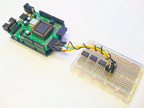
How much memory do you really need? We suppose it’s not really our place to judge how you misuse use memory in your projects. But we do appreciate the clean and orderly technique that [Eric Rogers] uses to add multiple SPI SRAM chips to an Arduino.
The heavy lifting is done with a CPLD shield called the Amani 64. It intercepts the SPI calls from the Arduino to an SRAM chip, and translates the address information to find the appropriate data on a collection of 23K256 devices. These chips are inexpensive, and using several of them provides a savings over choosing a single SPI addressable chip with a larger memory size.
The best part is that the flexibility of the CPLD allowed [Eric] to devise an addressing system that takes advantage of unused bits in the Arduino’s SPI data transfer functions. When using a single 23K256 chip, there are four write functions that waste a total of six bits. He devised a method to inject addressing data into these unused bits, allowing him to address up to 64 different memory chips for a potential of 2 MB of storage. The CPLD pulls out this injected address and subsequently writes or reads the bank of SRAM chips.
Looking for other SRAM upgrade options? Here’s another one that uses multiplexing to decrease the address lines necessary to add memory.


Wow, and “in my times” (i’m 22 :D) all you needed was couple latches. Maybe you youngsters :D don’t remember that some uCs (8051 anyone?) have a address and data bus avaliable on pins. One latch to demultiplex data from address and you have your 64kbytes worth of address space ready and waiting. Get something (latch toggled by another pin, i2c io expander etc.)to switch between banks and you can get yourself pretty much unlimited memory. And faster than serial too – if you go with latch method placing it somewhere inside address space you need only 1 write extra.
I have some of those chips here..
Can someone do a tutorial on storing video data from a cheap monochrome CMOS in one of these chips?
It would be ideal for doing data analysis on a stored frame, such as edge detection etc.
Essentially, store the frame for just long enough to do the edge detection, then store the raw data to PIC/AVR RAM and load the next frame.
Gets around the need to directly handle video data at full speed.
With all those pins available on the CPLD, wouldn’t it have been cheaper to make an SPI to parallel SRAM chip adapter? They’d be available in larger sizes.
To me, this is like getting a bulldozer to move your trash can to the curb. Not trying to be negative, but why a CPLD board just to access these chips? Now I am one for experimentation and learning, but seams like here we are using an Arduino (psuedo VM atop an AVR) atop a CPLD, why not just interface the AVR directly to SPI Ram, and forgo all the other stuff that slows things down, and is not needed?
Because then you’d have an AVR system instead of an Arduino? :)
Ok granted in theory that’s the same, but i think you know what i mean :)
brilliant -now for one to address DDR2,3 modules
So this speeds things up because you don’t need to juggle all the address bits of the larger memory – you just add a header to address which chip you’re talking with? This maybe a way of improving the performance of something like a video frame buffer. But if you need to do something like this then perhaps the base processor you’re using is a bad choice for the job in the first place. This might be more palatable if it used a $2 CPLD instead of a $25 Arduino shield with an Altera-Max CPLD on it (Quartas… shudder.)
Good points guys…. a few thoughts:
1. One reason for using the Arduino and Amani64, besides instruction, is for rapid-prototyping purposes, to quickly experiment before implementing a final design. Often the Arduino is dismissed as a toy, whereas it should be viewed a tool for a specific job; same as the CPLD shield. It should be a means to an end, for experimentation and proof, not the end itself. You would not deliver an Arduino and a stack of CPLD, motor driver and memory shields as a final product; you would however use the stack to perform proof-of-concept and initial software development THEN spin a lean board of your own with an appropriate bill of materials that meets your design specifications and price point.
2. This option demonstrates how to expand memory without expanding the I/O usage of the AVR. To address the additional memory chips the AVR would require a separate CS line for each 23k256. Using the CPLD commits only 4 lines from the AVR while the CPLD handles the bulk addressing/multiple CS lines. Admittedly it is a long way to run just to expand memory, just interface the CPLD to a parallel-interface SRAM and be done. However see point #4.
3. As described in the article this implementation does not add any delay to the actual SPI transfer; none that affects the AVR performance. tpd might be as much as 30ns here, however this will be unnoticed due to relatively slow Arduino SPI SCLK speeds.
4. Ultimately what I was hoping would be derived from this article is how to use programmable logic devices to intercept existing data streams and modify them transparently to downstream hardware. Something that might be of interest to the hacking community.
I enjoyed reading this comment even more than the actual hack. :) Good job, Eric.
Why use 64 chips to address 2 MB of ram when you can use that CPLD for a SDRAM interface. You’d get 64 MB of ram in a smaller package. Ofcourse, no breadboard prototyping possible. Or use plain SRAM.
If you don’t care about speed you don’t even need the CPLD, just a few shift registers connected to the memory pins.
All this CPLD + 64 chips looks like using a sledgehammer to turn on your TV. You can do it, you might be proud that you did it, but there are lots of better ways.
Nah…it is more like using a grenade to turn on the TV…completely pointless but if you can do it without destroying anything is an an impressive achievement.
I found it interesting to know that there is a CPLD shield available, I find that very interesting and I’ll be buying a couple to experiment with. thanks HAD // eric
640K ought to be enough for anybody.
Pfft, 128K is plenty!