We see a lot of projects using Eagle for the schematics and PCB layout. There are a few that use Kicad, but we hear very little about other alternatives. Recently, [Limpkin] has been working with Altium and Cadence and wrote about how they compare when it comes to PCB layout. Neither are free packages so it’s good to know what you’re getting into before taking the plunge.
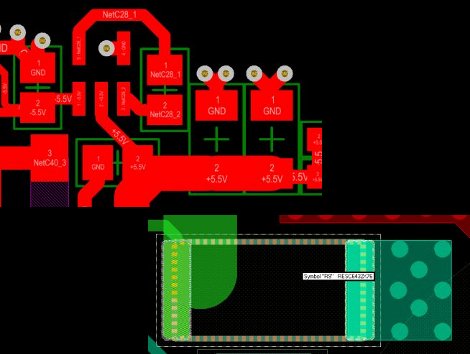
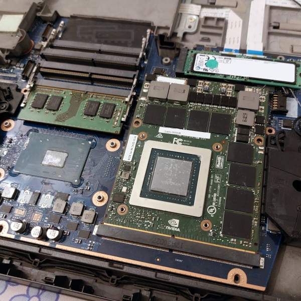
[Limpkin] begins his overview by mentioning that the schematic editors are comparable; the differences start to show themselves in the PCB layout tools. Here you can see that Altium always labels the pads so you know what net each of them belongs to. Cadence (whose PCB layout tool is called Allegro) will display the net if you hover over the pad with your mouse. Both have 3D rendering, with Altium’s looking a bit more pleasant but what real use is it anyway? Okay, we will admit we love a good photorealistic board rendering, but we digress. The most interesting differences show themselves once traces are all on the board and need to be rejiggered. Cadence will actually move traces on other layers automatically to avoid collision with a via that is late to the party, and Altium shows some strange behavior when dragging traces. [Limpkin] doesn’t register a final judgement, but the comparison alone is worth the read.


Ahem, would you by any chance be interested in some review of the DesignSpark package then?
Although it might be fairly new to the game and sometimes behave strange, I think that it has potential (as all the other programs out there)
“Both have 3D rendering, with Altium’s looking a bit more pleasant but what real use is it anyway?”
Ever made a case for a product?
Having just started using Cadence at work, I was wondering a lot what Altium was like, Thanks!
Over the years I have become adept with Eagle, then Kicad and now Altium.
For personal projects with limited complexity and limited impedance control concerns I still prefer Eagle or Kicad. These tools lack complexity which is great for learning how to layout PCBs. Having to do everything the hard way (like calculating impedance values based on the stackup, length matching signals, making foot prints, etc.) makes for fewer design errors in my experience. My advice for anyone who is doing a design that can be fabricated on the cheap is to stick with the basic layout tool.
Altium is very, very powerful and I love it and I hate it and I love it and I hate it. With that said; I could not do my job without it.
At the end of the day most engineers are stuck using the preferred tools of the company they work for. If you’re lucky enough to pick your own tools then stick with what you can afford.
– Robot
I would like to add that being able to export a 3D model of the PCB with components is invaluable. Also, a good rendering is very useful for catching mistakes before things go to fab.
. . . annnnd now years after this comment I am learning to hate Orcad and appreciate how wonderful Altium is.
They are all free to me, if you know what i mean
I’ve used Ultiboard, Eagle and some other free packages in the past. After Ultiboard I thought Eagle was fantastic (I had so much trouble with Ultiboard).
At an internship I met Altium and I loved it. Awesome program and as soon you get used to it’s very productive and all makes sense (it has a learning curve, but after 2 days you’re over that).
On another internship I had to use Eagle again. I was disguised. The move, copy, group tools seem retarded. 1990’s technology. “It’s a simple CAD tool”. iPhone apps are simple, and they don’t use such stupid user interface design. I really hated it.
However, I recently had to work with Mentor Graphics. Even worse! The copy schematic tool doesn’t even work. It had glitches everywhere, even messing up or ‘making decisions’ for your design. “Cannot short this net.” – what , I’m trying to connect a bunch of capacitors to GND?!
Horrible. Very often thought of Eagle being much better.
I’ve never encountered a company where I could choose my own tools.
You bring up my frustrations with any “smart” software. It’s like my co-worker told me “Altium is like a smart but stubborn butler.”
Mentor Graphics (DxDesigner and PADS in my case, by the way) did some thinking and it’s very annoying. Like the ‘cannot short net’. Or removing stitching via’s for no reason when I moved a polygon. Or the lack of ‘clarify selection window’. Nice when you try to match solder mask and copper shields.. it keeps selecting the mask layer e.g. while you are trying to pick the copper layer. Moreover, too fast clicking and it crashes.
I like it that altium has some Smart tools, like if you create a bus label DATA[0..15] and SmartPaste it with bus expansion, you can create labels, sheet ports, etc. of DATA0, DATA1, etc. Oh I need DATA15 on top instead? Press Y, and it’s flipped.
I haven’t encountered this ease of use in Mentor Graphics, Ultiboard or Eagle. Especially the last one involves lots of manual labor, which it so annoying.
Still though, using Altium does enforce some rules you need to follow. Especially in the PCB editor when moving traces around. I typically still delete parts, move and reroute.
Yes, Mentor Graphics was so horrid to work with. During one takeover here, the new company made use Mentor Graphics, as it was the “standard tool”.
It was super buggy and non intuitive.
We were then bought by a new company and now use Alitum, which is much better and a very powerful tool with lots of features.
BTW, i totally disagree with the 3D rendering being useless, if ya actually set of your part models to have 3D parameters, it is powerful. it will also dump a step file of your board so you can do mechanical fit checks. very useful and saved us countless times from fit issues.
(stupid report button, can’t hackaday put an confirm window on that?)
Yes, the 3D future is useful for mechanical design. In PADS it works kinda except you have to manually enter the height of most components at export (something about library management).
I encounted so many troubles, like I said in my other comment, with Mentor Graphics. Never again when I can choose (still a student)
I tried the ‘live 3D view’ in Mentor and it’s a joke. The render quality is like straight from 1998 when we had 8MB graphic cards. All components are basically cubes. That’s it. Seems like Cadence isn’t scoring much better, though.
With Altium you can place step files of battery holders and match enclosures to fit everything. It’s awesome.
I still have ‘learning a free 3D CAD tool’ on my to-do list just so I can make my own components and case designs. I know it can be of use later … :)
Of course the components are just boxes. You need to actually add the 3D models from the actual manufacturers.
Do that and you’ll end up with a pretty darn accurate representation of the board.
And to keep on going about Mentor Graphics.
The DRC rules is a joke. I only found minimum width and clearance. That’s it. You can set it up for groups, nets, but it seems troublesome.
The DRC check is even worse. Apparently it only checks area’s you are currently zoomed in at. Who thought of that?
Because of that, I was confused with inconsistent DRC checks and clarified the tool as ‘being mad’. So I did a manual check of the board. Which ofcourse is doomed to fail.
Result: 3 GND via’s shorted to an inner net, had to drill the via’s out and patch the inner nets.
And that’s a design package of several thousand dollars..
The people who work on huge boards with bajillions of connections?
I use PADS at work, and oh my God, I would wring its freaking neck if it wouldn’t do DRC checking on only a zoomed in area. That way you can correct areas one-by-one.
Also, PADS has a ton of DRC functionality. Rules specific for components, layers, nets, groups of nets. It’s not that easy to set up in Layout, but I don’t think Mentor expects you to use Layout for routing that much. It’s easy to set up in Router.
What I’d *really* like is if it had a “design-preference check” – where it tries to hit a design rule, but you can violate it if you push hard. I haven’t seen any software have a feature like that.
And the winner is…. vi!
I use Altium, and basically I think it’s great. 3D view can be very useful if you have stacked PCBs, are trying to pack connectors into tight assemblies, or have components or boards that overhang your main PCB (for example a card edge connecting daughter board over the top of other components). I’ve used Protel before that, which I also thought was pretty good (been trying to find a 2nd hand license for that for ages).
What I don’t understand is why there’s no cheap, highly restricted version of Altium. You could remove SO many of the features, limit layers and board size, and IMO it would still be a very useful tool. Anybody who used this would then be highly likely go on to pick the full Altium version going forward with larger commercial projects. How many people just starting out with an invention or other small scale project are going to pay $5500? Seems like a lost oppertunity to me.
True. Altium might as well not even exist AFAIC.
This has been discussed on some other forums as well..
The main argument against that is that *most* people use the Schematic capture and PCB routing tool. Most engineers may create 4 layer boards with like eurocard sizes (maximum).
Where do you set the limit at? Remove all the FPGA and Embedded stuff? Never looked at that anyway.
2 layer boards with 40x60mm? Well, is that even usable? Can you show off the benefits of hierarchical design and such in Altium? Probably to small design..
I’m for a free edition too. It would easily squash Eagle and other free tools. But they would lose commercial customers too, because the free edition probably does enough stuff to be sufficient for them.
I’m supportive of a cheaper no frills version of Altium. However, as Hans has said it has been discussed numerous times before, even in the Altium live forums.
At the end of the day, it looks like when the company listed on the stock market, they used lots of its new found capital to make a lot of acquisitions (FPGA in particular) and it has never paid off.
Apparently they are at it again, moving into the device ecosystem / internet of things space, possibly incorporating a lot more functionality into their product which I dare say the majority of the customers don’t want.
At the end of the day most of the customers want schematic capture and PCB, but unfortunately someone has to pay for the “vision” of the Altium’s leadership team. Let’s see if this new strategic direction pays off.
I’d love to see some Allegro tutorials! I’m having a hard time getting far enough over the learning curve to make anything useful with it.
There’s some pretty complete tutorials for Allegro on google. I teached myself with them for my last job.
Here is a link to our OrCAD + Allegro tutorial channel – http://www.youtube.com/parsyseda
Over 60 videos of OrCAD and Allegro doing all sorts of tasks with commentary.
I have been using altium for 16 years, mostly for dense RF/Microwave layouts. The DRC is indispensable when doing custom shapes and lots of via stitching. The 3D is also great for step exports; the mechanical guys love it. I wouldn’t touch Tormentor with a 10 foot pole, even though that is our plant standard.
Princess Cadence.
I used Hiwire, then Tango, then PCAD, then Protel 98SE, 99, Altium Designer 2004 and now summer 2009. I had to use Cadance at one job and quit because of it.
That all being said, I also have to learn The Autodesk design suite for 2d, 3d, 3ds max and so on (just to remain employable…it was either fire the mechanical guy and make the electronic guy learn it or fire the electronic guy and make the mechanical guy learn it…I won.).
For all sorts of great 3D components, electronic and other wise go to 3d content central dot com. I have uploaded parts, there is a very active community there. Great for those of you who don’t have access to a 3D CAD system.
I agree, I had to do a job in Cadence 4years ago. It was in transition at the time, horrible, and unusable. I ended up using Altium to get the job done.
Seriously? I’ve used Cadence, then Eagle, and now use Altium at work. Eagle is great for free, but Altium wins against both Cadence and Eagle hands down in ease of use. It just … makes sense. I think Altium is cheaper, too.
Nick Martin CEO and founder of Altium seems to have been kicked out by the shareholders – http://asx.com.au/asxpdf/20121015/pdf/429d1tpbcp23rj.pdf Not sure how this might change the product if at all
http://4.bp.blogspot.com/_oS8MUvla_vg/S4VN7uXauII/AAAAAAAACIs/aIU_JLKZ-7A/s1600/fig5a.jpg
Please can you tell me witch software is used to make 3D like this in image. Please I need answer.
Regards.
I have used both altium and cadence for years,. Altium – interface schematic capture to PCB layout -has cadence beat hands down.True , cadence has exceptional tech support– they have to support it–it;s so kludgy–always has been–they support it to keep the engineers committed to the other interfaces that are better than existing products. If Altium could break into the other interface areas, and be as organized and
competent as they are in the capture/layout arena they would blow cadence out of the water. I blow $20 K on that Cadnece junk and they just asked me for more. Thank you. If Altium gets smart, would there be stock available–it’s not in the American market- for me to purchase. –Sign me $20K behind the 8 ball…Gracias
i started with P-Cad Master Designer – then Accel EDA then P-Cad 200x and now Altium. Very powerful. All of our rules are input into the schematic. since Altium uses a “unified” database, the rules move to the PCB editor seamlessly. We can import geometry from our mech cadd tools and use that on the PCB. We then go the other way…. export a Step file and go back to our mech cadd for the mechanical assembly. Then it’s off to ANSYS for mechanical simulation. Speaking of ANSYS, we’re investigating the EMC/EMI analysis – imported directly from Altium. Supply chain and components…. WOW…. I’ve seen OrCad CIS and was impressed but Altium blows it away. Vaulting and version control, colaborative designing… many many more features. After you get past the learning curve you’ll never go back to a different tool…
I remember PCAD, that was superb back in the day. Altiums vaulting and version control is very good but to compare that with OrCAD CIS is not comparing intended functions. The OrCAD CIS was designed for three things, to place parts from an engineering database, to create extremely easy BOM variants from a parent schematic and to place parts from Active parts.com. This is what all the others try to mimic, such as PADS data book etc. CIS was the first. Most of the people I know already have a free vaulting and version control system that is used company wide and this means that you dont have to give everyone a seat of CAD to be able to vault, access and version control. With regards to 3D pretty much everyone OEMs Dassault Spatial. You watch what happens when dassault want an increase in per disc usage of their product, suddenly everyone will no longer have 3D unless you drop back to a previous version. At least a few of the ECAD vendors that have been bitten by this sort of thing before. Cadence and I think Zuken have written their own 3D STEP solutions (free in all levels of OrCAD and Allegro) , I must say Zukens looks really good too.
If you’re serious about 3D PCB layout, then Zuken’s Design Force has many more features and is rock solid stable. It’s not just a 3D viewer, you can actually design in the 3D view (2D is still supported). It’s also multiboard capable, so if you have two different boards in your design you can plug them together (or package and board) in 3D and route across both of them while still maintaining separate databases (allows you to optimize routing for the system). It exports and imports STEP files, but even better, it allows you to import the physical enclosure in STEP format and perform collision checks with the PCB and components.
I used Altium 3D design for designing flex PCBs and I think Altium has superior capabilities when it comes to determining the flex PCB’s bending radius. It also tells you how much you can bend before hitting the components on the surface you are bending towards. It is really awesome to work with and you can do a lot of things in Altium without going to solid works. Apart from that I have worked with Cadence allegro 16.6 and Altium 14. Cadence has a lot of issues sometimes which needs closing and opening of the software. I am seeing trends with many start ups using Altium as license is cheaper to invest and comes as a single package unlike cadence where we need to use orcad capture. The way schematics look and the hierarchy thing that you can do which Mr.Adam Fabio has done in his project files “A LOW COST ARDUINO FPGA SHIELD ” is simply cool and easier to go through schematic. Go Altium