Writing for Hackaday can be somewhat hazardous. Sure, we don’t often have to hide from angry spies or corporate thugs. But we do often write about something and then want to buy it. Expensive? Hard to find? Not needed? Doesn’t really matter. My latest experience with this effect was due to a recent article I wrote about the AM2900 bitslice family of chips. Many vintage computers and video games have them inside, and, as I explained before, they are like a building block you use to build a CPU with the capabilities you need. I had read about these back in the 1970s but never had a chance to work with them.
As I was writing, I wondered if there was anything left for sale with these chips. Turns out you can still get the chips — most of them — pretty readily. But I also found an eBay listing for an AM2900 “learning and evaluation kit.” How many people would want such a thing? Apparently enough that I had to bid a fair bit of coin to take possession of it, but I did. The board looked like it was probably never used. It had the warranty card and all the paperwork. It looked in pristine condition. Powering it up, it seemed to work well.
What Is It?
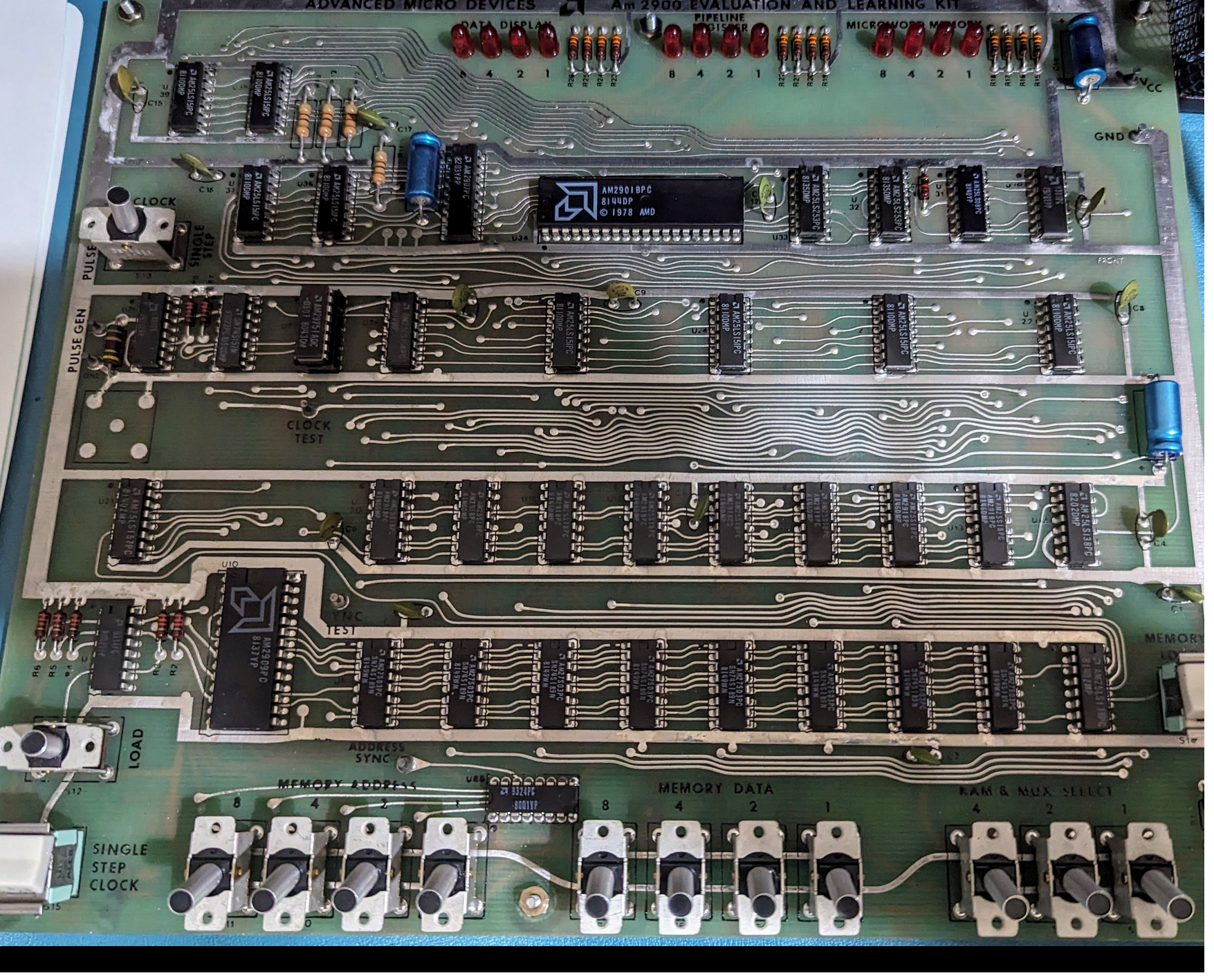
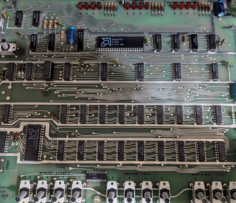
The board is a bit larger than a letter-sized sheet of paper. Along the top, there are three banks of four LEDs. The bottom edge has three banks of switches. One bank has three switches, and the other two each have four switches. Two more switches control the board’s operation, and two momentary pushbutton switches.
The heart of the device, though, is the AM2901, a 4-bit “slice.” It isn’t quite a CPU but more just the ALU for a CPU. There’s also an AM2909, which controls the microcode memory. In addition, there’s a small amount of memory spread out over several chips.
A real computer would probably have many slices that work together. It would also have a lot more microprogram memory and then more memory to store the actual program. Microcode is a very simple program that knows how to execute instructions for the CPU.
For example, suppose you wanted an instruction that added the A register to the B register and left the result in the A register. An imaginary microcode program might look like this:
Gate register A onto internal bus X
Gate register B onto internal bus Y
Set ALU to compute X+Y
Gate ALU output to register A
The microcode would normally also fetch the next instruction, too.
The kit lacks any program memory and only has 16 memory slots for microprogram steps. So, in reality, you can probably fake a single instruction and see how it works. But that’s about it. The example I’ll show you is a simple microprogram that converts an 8-bit BCD number into the equivalent binary number. That is, 2 and 8 will convert to 1 and C (since everything is 4-bit). Even this takes all the memory the device has. So don’t expect to emulate a VAX 11/730 (which did, incidentally, use 8 AM2901s).
How it Works
The board doesn’t have a microcontroller, so everything is ordinary logic. It is set up to work with 4-bit numbers and a 32-bit microcode word. Since board space and LEDs were expensive then, everything works with 4 bits at a time. The right-hand bank of switches (the mux select) lets you put a binary number from 000 to 111 (0-7), and that controls which 4-bit part you are working with at any given time.
The LEDs on the left show a data display. Exactly what this means depends on the position of the mux select switches. For example, when the switches are at 001, the data LEDs show the output of the ALU. When the switches are at 010, the ALU’s flags (for example, carry and zero) appear.
The other LEDs show four bits of the pipeline register — the instruction the board is about to execute — and the contents of the microprogram memory (again, the selected four bits).
When the Run/Load switch is set to the load position, you can enter an address on the left-hand switches, and data bits on the middle switches. Then you press Memory Load. That means to completely enter a 32-bit microinstruction, you have to flip the mux switches 8 times and then enter each 4-bit value, one at a time.
If you flip to run, you can use the single step button to execute an instruction, or you can hook up an external clock and use that.
This is all confusing to read about, but the video below will help you see how this old hardware works.
Internals
Internally, you can see that the microprogram memory feeds the pipeline register. The address is from a multiplexer that can select an address from several sources. The pipeline register provides 32 bits that control everything from what the next address is to what the ALU does.
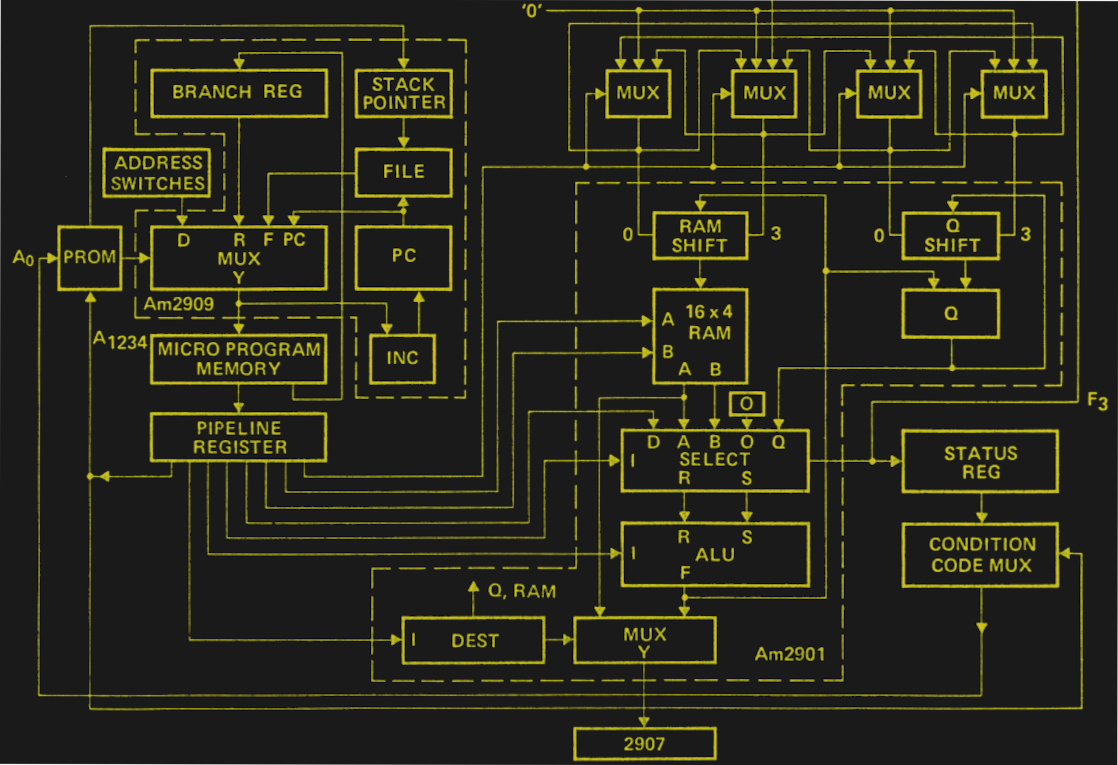
There is a small PROM that serves as a lookup table to control the sequencer. This allows the instruction to use a small number of bits to control the AM2909 sequencer so that you can select the next address, have conditional jumps, or even push or pop the stack internal to the device.
Essentially, the sequencer decides what word to execute, the AM2901 does most of the execution, and the rest is just memory and a little glue logic.
In a real system, you have to account for things like the carry flags and detecting a zero result. However, having only one slice makes things easier. The carry input is part of the microinstruction so you decide when there’s a carry and when there isn’t.
Microinstructions
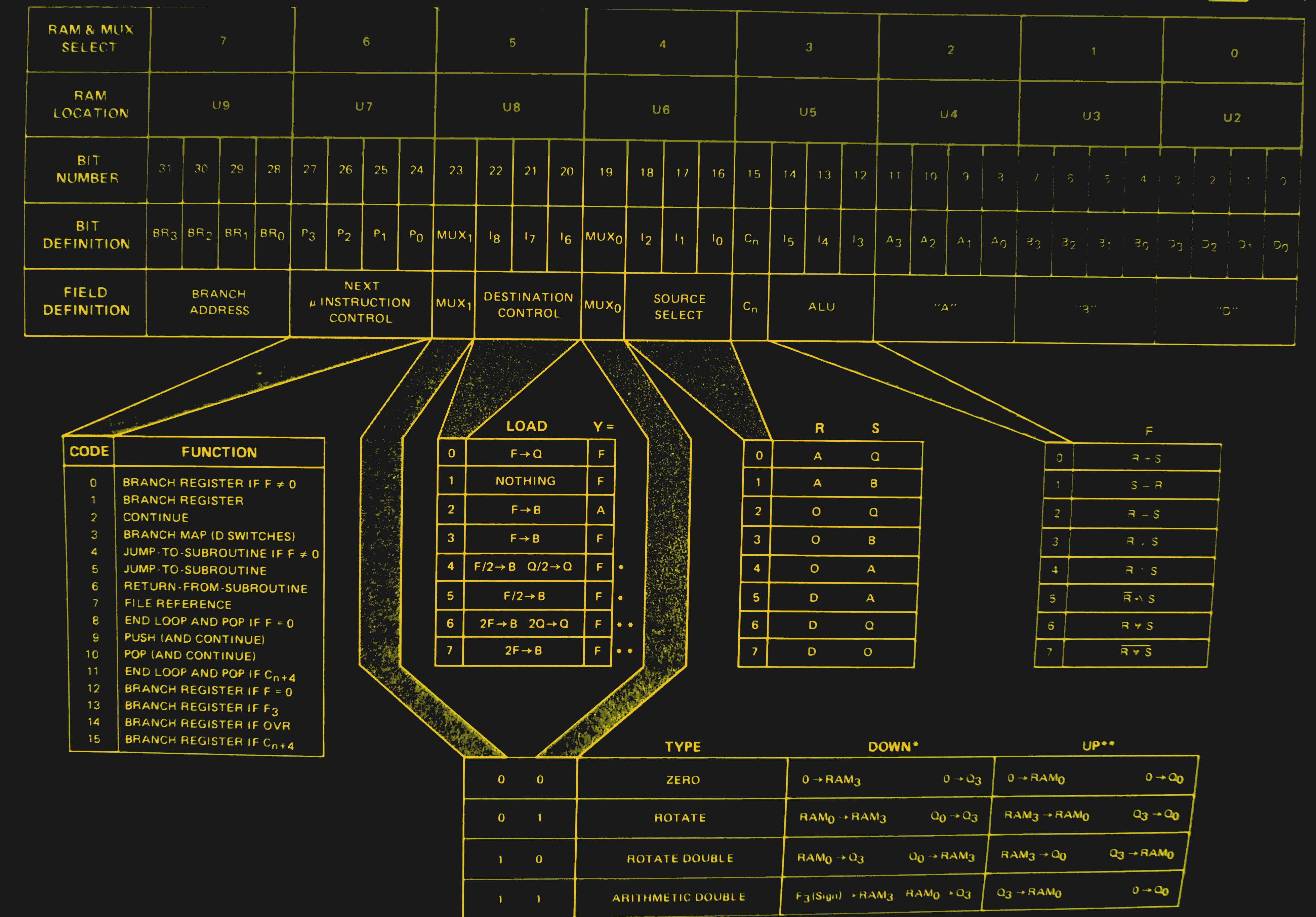
In a real design, the microinstruction size and format were totally up to you. However, since we are using the evaluation board, you must use that format (see the figure below). Each instruction had several major parts: a way to specify what instruction would happen next, a source, and a destination along with an operation. In addition, there were two register fields and a data field (all, of course, four bits). Not all fields are used in every case.
This is a very flexible arrangement because you can, for example, do adding, shifting, and a conditional jump all in one instruction. However, it can take some getting used to. For example, loading a register is usually done by using a logical OR instruction with a constant zero.
The other thing that is strange is the pipelining. Because everything is set up at the start, a conditional jump doesn’t apply to the line it is on but the line before. For example (in pseudo-code):
Goto next, set Q to A+1
If zero goto bump, set B to B+1
The “if” in the second line will trigger on the addition done in the first line.
Assembler
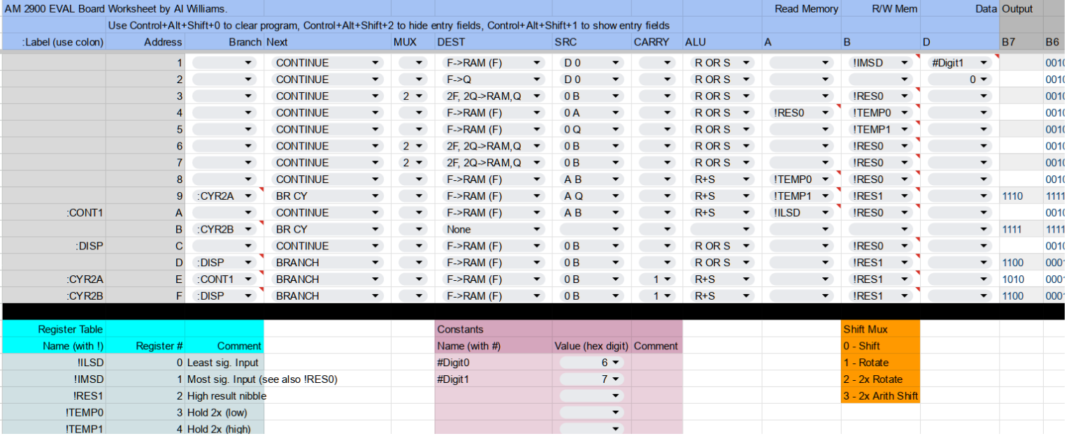
If you watch the video, you’ll see that entering a full program is tedious and error-prone. To help, I created an “assembler” using Google Sheets. You can use symbols for addresses, registers, and constants. In most places, you can use a drop-down to pick among options. There’s a place for comments, too.
Once it is filled in, you can hide the “source code” using Control+Alt+Shift+2. That gives you a handy piece to read or print for putting the data into the board. Control+Alt+Shift+1 will restore the display.
| Address | Branch | Next | MUX | DEST | SRC | CARRY | ALU | A | B | D |
| 0 | CONTINUE | F->RAM (F) | D 0 | R OR S | !ILSD | #Digit0 | ||||
| 1 | CONTINUE | F->RAM (F) | D 0 | R OR S | !IMSD | #Digit1 | ||||
| 2 | CONTINUE | F->Q | D 0 | R OR S | 0 | |||||
| 3 | CONTINUE | 2 – Double | 2F, 2Q->RAM,Q | 0 B | R OR S | !RES0 |
Consider the excerpt from the demo program above. The branch column could contain the next address to execute, but since each line has a continue, the address can be blank. The system will ignore it anyway.
To the right are the A, B, and D columns. The A and B columns are numbers from 0 to 15 signifying one of the ALU’s internal registers. Here, we don’t use A, so it is blank. The D field is for a four-bit constant if you need it.
The ALU column holds the operation to execute and the SRC column is what the inputs to that function are. In the first line, for example, we take D and OR it with zero. At address 3, however, the OR is between a zero and the contents of the B register.
The DEST column tells where the ALU result goes. In most of these lines, it goes to RAM, which is the register named in B. However, at address 2, the result goes to the Q register, which is internal to the AM2901. The destination for address 3 stores the result after doing a double (that is, 8-bit) shift to the left.
Obviously, a lot is going on here. If you want to know all about it, you’ll need to read the datasheets and the board manual. I’ve left those for you over on Hackaday.io. You’ll also find links to the assembler and some other material there.
Don’t have a board? No problem. I’ll make an emulator — also spreadsheet-based — available in the next installment along with more about the chip’s internals. If you missed the post that started me down this path, you can go back and read more about the internals and the device’s history. There are plenty of emulators for machines that used the AM2901, although they probably mimic the behavior, not the circuit.


Nice find. Reminds me of the NorthStar “hardware floating point” S-100 board I had years ago. It used a microcoded 74181 :-) And Polymorphic BASIC could make use of it. Quite an impressive speedup.
Neat!
My first microcoded processor (uni project) had 64 microcode points and four 16bit registers available. It was sufficient, as the program counter was treated as a regular register (other than incrementing on each instruction) and all loads were conditional. IIRC, there were four instructions, one of which carried ALU control bits to allow the full suite of logic and arithmetic.
In silicon mid-80’s.
HP1000 21MX -M, -E,-F systems were based on the AM2900 bit-slice system for their cpu board and floating point hardware. It was micro-programmable and had a lot of special instructions. It used 4 AM2900 on the CPU board with the micro sequencer for the microcode.
LEDs were expensive back then? On what planet? I was buying ’em with my own PeeWee Herman/Chris Elliott newspaper route lawn mowing money. They were after all, diodes. Might as well say the switches were expensive. Bright side, aesthetically it’s a beautiful device to this reader.
All relative and if you are designing at scale and not buying hobby surplus it counts. I don’t know exactly when the board was designed, but a quick look through an old catalog from 1973 showed Sprague LEDs running from a buck and and half up to about $6 each (more for strange ones like IR). Plus in 1973, $6 was a lot more money than it is today.
When the cost of a single LED was comparable to a 100ct box of incandescent lamps. They were considered expensive.
In the early 80’s we were doing a bit slice ramdisk controller (Dataram BC-901) that used 4X 2901, 1X2910, a bunch of fast INMOS X4 SRAMS (35nS!), and PROMs (uCode).
A California company called CCT built an IBM1800 emulator based around the 2901 and a micro sequencer. Pretty impressive. It was first used by the USAF. A version of it controls a CANDU reactor in Pickering, Ontario and is still operational.
Great article. Next project for you: TMS1000 masked programs, accessed by Test Mode ? That wo uld be kool iff you did it.
BTW Part of the tkgate simulator is an microcode assembler called gmac. It can be used to programm sequencer as well as alu and rest of the logic, very close to the original 2901 AMD assembler.
Brings back memories of working at a desktop computer manufacturer. The ALU was two 74181 24 pin chips controlled by microcode on ROM.
https://en.m.wikipedia.org/wiki/Datapoint_2200