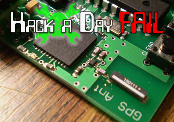
GPS is really fun to play with in your projects. But when [Trax] decided to build a GPS chip into his design the fun ended abruptly. Above you can see the section of the board devoted to the hardware. Unfortunately this PCB fails to provide any GPS location data whatsoever.
His design uses a Low-Noise Amplifier between the Venus634FLPx GPS receiver and the antenna. After populating the board he was getting no satellite fix. He tried replacing the antenna, and also two different antennas connected without the use of the LNA. He could get NMEA data, but still no fix. After checking and rechecking he finally went to the chip manufacturer for advice. They came back with some helpful suggestions, but he’s bogged down in trying to figure out if there may be problems with his antennas, and with the need to spin another PCB to test some of the proposed fixes. Take a look at his write-up and leave a comment if you see something that he might have missed.
Even working with develpment-board-GPS hardware has its ups and downs. [Jeremy Blum] tried to track his possessions as they were moved across the country in a PODS container. As a Fail-of-the-Week extra, check out how his hastily assembled tracking hardware failed to work past the first few hours of transit.
 Fail of the Week is a Hackaday column which runs every Wednesday. Help keep the fun rolling by writing about your past failures and sending us a link to the story — or sending in links to fail write ups you find in your Internet travels.


Wow, so now somebody’s failure in designing a board is worth an audience of thousands of people?
Yes,
Its a teaching moment for others.
In many ways. He was quite a tool in panning the device when they went out of their way to help. He caused the failure and blames the device.
That’s not really what I took out of this. The way I understood it he was saying that a problem with the chip was just one of the possible things wrong with it.
I also agree with BJ. The whole point of Fail of the Week is to shed light on problems, even if they’re self caused. This sort of thing is invaluable for learning how to take your design from datasheet to board layout.
Hi guys, thanks for your comments, sort of :-)
In the article it is clear that I made mistakes in my PCB design, so when I say “don’t go for Venus chip” I mean “don’t go for Venus if you are not 100% sure about its RF front-end”.
If I remember correctly, their datasheet stated “Do not connect GNDRF and GND” but external LNA’s GND should have been connected to GND and that’s the confusion I had. Keep in mind that in 2009 this chip was still “new” and there were no clear reference designs.
Anyway, I updated the original to avoid the confusion.
fartface is one of the top HaD trolls don’t pay him any mind.
I do some RF layout for a living.
I noticed one thing, the RF ground on the venus chip does nothing but connect the ground pins together on the RF side. There is no GND for the RF GND pins on the venus part. He could try jumpering to the LNA from the venus part as there is a ground pin on the venus part right next to a grnd pin on the LNA. It won’t be a good as a proper RF ground, but it will be a ground and might get things working. (When they say don’t connect GND to RFGND it doesn’t mean total isolation. What you want to do is have the two GND planes connect in a single point (50 mils is a good starting point) . You also want the power supplying the RF components flowing in over this point on an adjacent layer.)
Also I don’t know what LNA he is using but the reference designs are not always for the freq you want. And when he grounds the LNA he wants the ground via as close to the GND pin on the LNA. For his decoupling caps on the LNA he wants to keep the path to the power and ground pins as short as possible. Extra length of the power and ground paths to the capacitor increase the inductance of the path reducing the effectiveness of the capacitor. Also he may want to consider blowing away the thermal reliefs to the capacitor connection to the ground plane for the RF side as they increase inductance to the capacitor as well.
My sole purpose for reading this entry is because I’m in the middle of my first wireless design, and I’m trying to avoid failure by reading about this one. Case and point.
It is disappointing that he says “If you have even the slightest doubt, don’t go for Venus GPS.” when the manufacturer went out of their way to troubleshoot his design.
Yeah, if the supplier supports you & their stuff can be made to work for others you can’t really bad mouth the supplier for your own shortcomings.
Yes, but if it is hard to get the thing running, than it is not wrong, to tell beginners not to use it.
I can’t tell if he’s being unfair, or just worded it poorly. Perhaps what he meant was “if you have even the slightest doubt about what you’re doing with microwave RF design and layout, don’t use a bare receiver chip like the Venus.”
Use an existing module, designed by someone who specializes in this particular area of expertise. And if you want to try making your own, at least make it a separate module; so that it can be individually revised and replaced if needed (and it probably will) without making a much larger board useless. Once your module is working adequately, it can be integrated into the main board on a later revision.
Ah, now I see what is getting under the skin of some readers. I assumed he meant don’t go for a bare chip if you don’t know what your doing (like Chris explained), rather than saying avoid this manufacturer.
How is this a bare receiver chip? What else does it need besides an antenna? It has a integrated LNA. Just because he isnt using it isnt the manufacturers fault.
“What else does it need besides an antenna?”
If you bother to read the application notes that come with these modules, you will see that they also “need” a very careful board layout that may require multiple iterations before it works well. Even if you have all the parts you “need” it’s not going to work unless you follow through and get it all right.
Also if you plan to actually sell your design then you will “need” to get FCC approval for it. If you use a pre-made module they’ve already taken many of the necessary steps.
So basically it needs what I all ready said? Thanks Mr. Obvious.
No, seriously I tried the Venus and had the exact same problems. The chip just sucks and appears to be poorly designed. I tried to get support as well and not any help just said refresh firmware and crap. I also got the impression that they were kinda the bottom feeders of the GPS industry.
My tip would be FOLLOW THE DATASHEET TO SPEC. The writeup mentioned not 1, but 2 instances where the designer did not follow the specs for the design. Follow the directions stated in the datasheet before complaining to the company. And don’t blame their unit before following the design to specification. They don’t just publish those for the fun of it…..
I would go even further and say that you should go for a pre-made module that’s already had these difficult RF issues debugged. Even with the spec sheet a lot of this stuff is “magic”
Reading a datasheet fully is a problem. You don’t need 90% of the info in the datasheet. There are pages and pages of graphs about power-usage on voltages you’re not using. So you normally read the parts of the datasheet that you think you need to know about.
A few days ago, I ran across a guy who used a chip. The (mostly 12V powered) chip provides “5V” for decoupling, but also for “limited” use outside of the chip. Neat! The “reset” line of the chip doesn’t officially need to be pulled high, but it’s best not to leave it floating, right? So this guy hooked up the reset line to the 5V output of the chip. Turns out the reset line being low resets the chip, including the onboard regulator. So the chip wouldn’t bootstrap…..
Another case I just stumbled upon. In the STM32F4 chips, if you disable the internal reset circuit, you suddenly lose “vbat” operation. This is burried somewhere in 2000 pages of documentation on the chip. Are you going to read all 2000 pages of documentation before you finish designing the board? I sure as hell didn’t. Boards are coming in today. :-)
If there’s already fine pitch SMD on the board, why bother with the ugly DIP MCU ?
Street cred, so it looks more like a freaking arduino so he can say it is arduino compatible -.-
it didnt work because the GNDRF is not connected to anything. And he assumed that just using the normal GND for everything would be enough.
the 1st advice from the manufacturer should work, not ideal. but should get him readings
Wow he went the long way around to track his stuff. Cheap prepaid phone + arduino. one of the older low end nokia tracphones exposed the gps out the rs232 on it’s connector and modem commands to sen a text message.
Wrong post. I guess we get 2 fails this week!
When fartface fails, we win!
Uhm..
This “fail” was done in 2009. (zzzzzz)
Yes, but someone could still make the same mistake in 2013. (hmmmmm)
So it was a good read anyway…
apparently failure has to happen on schedule
” and with the need to spin another PCB to test some of the proposed fixes.”
Really? A new PCB for every change? Why not just get a Schmart Board or something similar, prototype the RF stuff Manhattan or Dead Bug style, Breadboard the rest? Once he has a proven working design, then neaten it up on a custom PCB if that is even necessary.
Etching a custom PCB for a design you have never actually wired up before sounds like a perfect recipee for frustration and failure to me.
“Why not just get a Schmart Board or something similar, prototype the RF stuff Manhattan or Dead Bug style”
Prototyping RF stuff that way sounds like a better recipe for failure to me :)
+1
when it comes to high frequency RF (or RF in general) forget about Schmart or breakout boards…
And go straight for deadbugging on copperclad with a healthy dose of Kapton, kids.
^^ THIS ^^
^^ that ^^ plus copper tape and coax.
Copper tape over kapton (over ground) can be used as power plane(s).
Coax can be use where you need controlled impedance. I used coax as
200ps delay line that save our proto when the vendor changed the specs
on us.
The only problem is that once you get the proto working deadbug style,
you still have to do the hard work of doing a proper PCB layout if you
are churning out widgets. PCB as in striplines/microstrip etc are also
components in a RF design that are not tested on a deadbug.
Multilayer microwave mixed signal boards can be manufactured with first pass succeses without wiring up the circuit. I do it all the time. It takes engineering and experience, not hacking. Of course everyone wants instant gratification these days so engineering and experience are frowned upon.
The GND and RFGND are separate since bond wires inside the packages have inductance. You don’t want a noisy MCU pulling current through the same bond wire as your RF signal. Doesn’t mean the can’t be hooked together at some point. GND is a mathematical common node; it does not exist in reality.
Not quite. They’re separate because *distance* has inductance. Not just the bond wires. That is, if the return current is forced to travel way far away from the signal path, you’ve got a huge inductor – draw the current path, and you’ll see a big loop. The RF section is at GHz speeds, and is a controlled impedance, so it needs to have the *right* inductance back out. Which means you need a ground path at the right spacing from the signal, and usually *bunches* of them to help direct stray low-frequency return currents – you can kindof think of that as like a Faraday cage.
Should GND/RFGND be tied together somewhere? Yes! They almost always have to be! If they’re not, there’ll be some potential difference between them due to whatever the effective impedance is between them, and if that difference is high enough, the return current will say “screw it, I’m going through this other path” and at best things start working worse. At worst, the chip can be destroyed.
“Why not just get a Schmart Board or something similar, prototype the RF stuff Manhattan or Dead Bug style”
lol that was the funniest comment ever!! laughed really hard.
RF stuff is not like wiring an arduino.
When you’re working in RF frequencies there are a lot of things that you have to consider. Things like trace width, right angle vs curved bends, whether you have a ground plane behind the signal line, the length of the signal trace (impedance matching is a bitch)… PCBs are pretty much the only way to get any kind of consistent results out of an RF system.
Exactly. Especially when dealing with signals in the GHz range. (GPS signals are around 1.2GHz, or a wavelength of about 25cm). You can really only breadboard, deadbug, or manhattan style build consistently up to a few tens of Mhz, or wavelengths longer than about 10 Meters (convieniently the upper limit of HF). Getting any smaller than that, and your parts, wires, and traces start to become a significant fraction of the wavelength, and a relatively minor change in their length or seperation will make a major change in the tuning of the circuit. A PCB makes these things much more consistent, and this is also part of the reason we can consistently go higher in frequency now than say, 25 years ago. As our components get physically smaller, it is easier to go to smaller wavelengths.
Sorry, just have to be a picky bastard. GPS is at 1575.42 MHz with a wavelength of 18 cm. To make it even trickier, the signal has a bandwith of between 2 an 20 MHz depending on your application and a power level at the antenna input of around -130dBm.
You play this game by the vendor’s rules or struggle in vain.
For those that are interested here are a couple web sites I use for a few RF calculations.
http://people.web.psi.ch/gaspar_m/cgi-bin/rfmwtools/rfmwtools.html
for a grounded coplanar wave guide I use this. It should be set with a good starting value for 1.575 GHz using 0.062″ thick FR4 plated with 1 Oz copper.
http://tinyurl.com/n239lhd
Thanks for the links! very helpful and useful.
This site was moved to: https://rfmwtools.web.psi.ch/rfmwtools/rfmwtools.html
It seems the biggest fail here is the stream of negative comments :(
I was really looking forward to seeing the fails and how they were fixed (if they were) but it turns out that it’s just a troll magnet.
Apparently this RF stuff is pretty…… polarizing to the audience
*puts on polarized sunglasses*
YEAHHHHHhhhh!
It’s those damn grey beards that make them cranky, plus a couple people talking smack without knowing shit about RF (can you spot them?)
Speaking English friend.
Troll = Arsehole
I agree. The smug-o-meter appears to be pegged in some people.
The PODS tracker needed an accelerometer connected up so the rest of it would power down to sleep mode when it wasn’t moving. Bump the accelerometer, wake up the rest of it, try to get GPS signal. No signal, shut down for x amount of time no matter what the accelerometer is doing.
After that wait, check again for GPS. No GPS? Wait again for accelerometer, if it says “Hey, I’m movin!” (obscure video game quote there) check GPS again. Got signal? Return to regular operation mode – else sleepy time again.
(Game quote is from one of the Terran ships in “The Outforce”. It could’ve been a great RTS if the publisher hadn’t forced it out the door unfinished. I loved the unlimited group sizes so one rightclick could command an attack of 100+ ships.)
An accelerometer would have been a suitable option, but lacking such hardware you could just increase the time interval between the attempts to acquire a GPS and GSM signal. After 3 attempts, sleep for an hour or so before trying again. The next time a signal is acquired, reset the interval to a few minutes.
I have a commercial GPS tracker that fails in exactly the same way; inside a metal shed, it will drain it’s battery in a matter of hours, while it normally lasts for a few weeks.
I suspect that this design could be working very quickly with a tiny bit of effort. Ive had very good luck with the skytraq chips. He can use a short length of wire as an antenna curled to the right hand’s fingers direction (if the thumb is pointing up). The LNA is not essential. What is essential is either using GPS Utility to load the ephemeris into the chip from the network beforehand (AGPS) or letting it run for *quite some time* without disturbing it to get the full ephemeris before it starts acquiring satellites. It should also have a backup battery attached. In my experience, a backup battery makes all the difference to system stability. And he should read up on the separate RF, DC and digital grounds with skytraq. Once he gets this figured out his GPS will sing. I would strongly suggest using, as the other poster said, a large RHCP square GPS patch antenna, ideally with a ground plane of some kind beneath it. See the “Antenna Evaluation” page at http://translate.google.com/translate?prev=/language_tools&u=http%3A%2F%2Fgpspp.sakura.ne.jp%2Fanteva%2Fanteva.htm for ideas on what works best.with cheap RTK-capable hardware (like Skytraq’s S1315F chip). That should also work best with a conventional GPS like the Venus 6.
This might’ve just been a mistake in the old datasheet: he says it says “This I didn’t do as their datasheet clearly states “Do not connect GNDRF and GND” and I was not sure that my LNA could be powered through the GNDRF from Venus634FLPx.”
The current datasheet (on Sparkfun) doesn’t say that anywhere. The example schematics do the goofball thing of splitting off an ‘analog’ and ‘digital’ ground (and connecting them with a 0 ohm resistor) which, in my experience, has only ever caused problems by people not understanding analog/high-speed digital design. (Short answer: don’t split a ground plane ever unless they’re not actually at the same potential. It doesn’t do what you think it does. Just use a single, solid ground plane. Especially for prototyping.) At best, it does nothing. At worst, someone forgets to actually connect two grounds that should be connected, and it flat out doesn’t work. (See this example!)
In any case, it looks like a 2 layer board without a solid ground plane on the back. That’s the big problem. In designing any 2-layer board with signals above, say, 100 MHz, make the back a solid ground plane, and treat routing traces there as an absolute, violent, awful last resort. You’re better off creating jumpers on the top layer or using bunches of 0-ohm resistors to create space than routing traces on the back.
I beg to differ on your opinion on never splitting ground planes. A split ground plane can make the difference between a circuit that works and one that doesn’t. In the last RF board I designed we had CPU interaction with ram RAM that clobbered our low phase noise oscillators even though they were three inches apart and had a split ground plane and a shield between them. On the next proto rev we moved the connection point between the two planes doubling the ground path length between the two areas and absolutely killed the noise problem.
The reason for splitting a ground plane is so that portions of a subcircuit can effect the ground potential in its locality without effecting other near by subcircuits ground potential. In some cases split ground planes are essential even on prototypes. If we had a solid ground plane on the first proto we wouldn’t have had enough isolation to even diagnose the problem by reducing the RAM interface signals’ drive strength.
Not every circuit justifies the use of a split ground plane but when you don’t know how noise will effect things its always a good practice.
If you’re having issues with your CPU/RAM signals traveling over 3 inches out of their way into a split plane’s ground then you’re doing something wrong. My guess is that either the CPU or the RAM doesn’t have enough localized ground vias (or bypass capacitors with localized vias) to handle the high currents generated by the high speed digital switching. You can mask over the problem like you mentioned (discourage ground returns through areas by moving them farther away electrically) or solve it entirely by making sure you have good bypassing/grounding on each end. Solving it is going to be best since you’re probably on the verge of having ground bounce/supply ripple problems as well.
I’ll offer a counter opinion. If you don’t know exactly what you’re doing then design your multi-layer PCB with 1 layer dedicated to ground. I mean everywhere. Liberally drop ground vias at every IC and make sure your bypass capacitors at each IC actually have their own vias too. Then sprinkle in extra vias to tie all of the extra copper between the different sections on your PCB to ground as well. You can solve the ground “noise” issue by guaranteeing the straw signals in your circuit always have a shorter path.
“If you’re having issues with your CPU/RAM signals traveling over 3 inches out of their way into a split plane’s ground”
Exactly. This is the thing I never understand when people talk about splitting grounds. The return current of a 100 MHz signal is constrained to a fraction of an inch underneath the signal due to inductance. It’s not going to go bother an analog signal 2 or 3 inches away, regardless of whether or not there’s copper joining them.
In fact, if you’ve got a setup that’s sensitive to the location of a join in a split plane, it’s probably because the plane split is a slot antenna and you’re picking up radiated noise. In which case the problem would *go away* if you got rid of the split entirely.
The CPU’s 620 ball bga has far more decoupling caps and pwr/grnd vias than the chip mfg recommends (in some cases as many as three gnd vias for a pin). The same goes for the 266MHz DDR2 ram chips. When you guys can do 64-QAM in in a 6.25KHz radio channel and go 10 miles getting better than 56K bits per second, and have an actually measured receive sensitivity of -117dbm (not just quoting a chip spec sheet) at this speed I’ll listen.
Just simulate it if you doubt me. The ground coupling of a 266 MHz signal is not going to go multiple inches away. The return current density there is nothing. Moving the tie point probably moved where the noise coupling in from the slot antenna was concentrated.
And puffing out your chest on the internet? Seriously? You have no idea who you’re talking to or what they’ve done previously. Your two examples were a split ground plane with a tie close to an analog component, and a split ground plane far from an analog component. Did you try a solid plane? If you did, and there’s still problems, the problem is probably that the design is space-constrained, so you simply can’t put enough distance between components. *That’s* a reason for moats in the ground plane, but again, that’s something you do *after* a design doesn’t reach initial goals. Not as a first step.
Hardware in hand is worth all the simulations in the world, that is why they still make dev boards. It also wasn’t 266MHz that was the problem it was the power used by the burst reads that created noise around 20MHz. Furthermore space constrained the design was but getting it to fit in an existing case saved the customer $50K having a new die casting mold made for the case and provided another two months time to market savings.
Patrick,
May not know what you have done but I can tell you that your attitude and design philosophy won’t cut it in a world where each board spin can cost over $10K per prototype cycle when you include documentation and labor costs.
Looks like I can safely say that there’s going to be no agreement here. Sounds like a good case to point out that boards like this can take multiple board passes to get “right”. Let me revise my earlier comment for those reading this thread with the intention of learning.
School of thought #1) Make bypassing easier for local signals. If you’ve got high-speed signals going inches out of their way and you can detect them (or their harmonics) with equipment (spectrum analyzer, etc) several inches away then there’s a reason for it. Figure out why they’re going so far away and fix it. Reasons can include: Improper power grounding, improper connection to power planes, high speed switching signals, improper bypass capacitance values (real capacitors have inductance too!), etc. Find out where the current path is and give it a shorter option. A 20MHz signal can travel several inches if you’ve got crosstalk problems, capacitive coupling into nearly high impedance lines, etc. Figure out where it is and give it a lower impedance path back to its source.
School of thought #2) Make it harder for the noise you’re generating to get into places where you don’t want it. A split plane can do the trick since you’re enforcing physical separation. Moving the ground point farther away from a noise source helps. This can take plenty of care to do to avoid negative side effects like those listed above or discontinuous ground returns.
Remember everyone — current always flows in a loop. You can give it a better loop (#1 above) or put the items you care about into a loop farther (electrically) away (#2).
Think about it like you’ve got two uneven resistances in parallel with each other. The smallest resistance is going to conduct the most current. However, the higher resistance is going to conduct some too. It all depends on the ratios of the resistance you’ve picked. #1 above is trying to measure the current through both resistances when one of them is ~0Ohms. The other resistance doesn’t matter since it’s paralleled with ~0. #2 above is trying to increase the impedance of one of the resistors to infinity. In this case it ceases to matter and the dominating factor is the other resistance in the circuit. You can heavily impact the performance of the circuit by tweaking to either extreme.
Make a more optimum path or get the items you care about farther away.
Let me be clear here: when I say “split” ground planes I mean completely disjoint copper pours, with some external tie (i.e. a 0 ohm resistor or, frequently but much worse, a ferrite bead). There is virtually *never* a reason to do this – the external tie is just a very, very dangerous point of failure, and you’d be better off just joining the copper pours. Adding inductance to the tie point (with a ferrite bead) is very dangerous, depending on what its resistance is, and at best just pointless, because the diversion you’re forcing any return current to take is already a huge inductance.
You can still steer stray low frequency return currents away from sensitive portions of the circuit with gaps in the ground plane, but of course that means *no* traces crossing those gaps at all such that their return currents would try to jump it. This is still dangerous, and should only be done if it’s found that it’s necessary, *not* as a first design. (See http://www.analog.com/library/analogdialogue/archives/46-06/staying_well_grounded.html for examples).
However in almost all cases you can fix any problem which you *think* needs a split ground plane by paying attention to the return currents, reorganizing the circuit, or possibly adding an additional ground pour to guard the sensitive portion.
I was told to look at the conductive EMC of a PCB that a group in a
different campus designed. They had a split plane where as our campus do
not split ground planes.
My intuition told me to short out the split with a solder wick at the
point to the backplane and was able to show the different of the before
and after picture on a spectrum analyzer. It confirmed that the ground
split was forcing the current to go to the worse possible direction.
i.e. forcing the ground path to go around a few of a high current DC/DC
converters where it picked up noise instead of straight to the back
plane ground.
I guess the practice of splitting ground plane came from the single or
double layers days. Unless you know exactly what you are doing, on a
multilayer board you are better off not splitting the ground plane.
In one of the previous posts this is mentioned:
>Another case I just stumbled upon. In the STM32F4 chips, if you disable the internal reset circuit, you suddenly lose “vbat” operation. This is burried somewhere in 2000 pages of documentation on the chip.
Yes, now I remember this. There is a similar situation with skytraq. You attempted to make the whole system run off on one DC source and failed to include the small backup battery or supercapacitor. This is easy to fix, ex post facto. You should be able to add a small lithium battery to hold the temporary data. Also, break out the reset to a test point and add a separate reset button if you need it. You can use a bypass capacitor to connect the RF ground so your antenna functions properly. Without a ground/shield its just an expensive inch long piece of wire. It cannot work properly.
First of all, it’s really cool that Venus was willing to troubleshoot that design — especially since it’s obviously for low-volume production.
For anyone new to RF: start by following app note/datasheet directions to the letter — I know it might seem pedantic, but I’ve seen RF designs completely fail to work altogether simply because of some minor layout issues.
Specific to this board, I see a few funny things that Venus didn’t mention or elaborate on:
First of all, more thought needs to go into your capacitor/via connection style. Try to put capacitors between the via and the pad — don’t put a via right next to a pad and then on the other side of the via, route a trace to a capacitor. Secondly, the “ground” side of the capacitor shouldn’t just go to a plane — it should go to a plane and a via. This will ensure a good grounding connection.
Secondly, this design has some funky polygon pours going on — there should be plenty of clearance between the RF and the top pour; remember, it’s a transmission line, so if the poly pour is too close, the capacitance of the trace will be too large. I tend to shoot for 20 mil RF traces and about 25 or 30 mil of clearance to the nearest polygon pour (though, obviously professionals would calculate those values based on the desired feed impedance, given all the board’s parameters like copper weight, thickness, substrate material, etc)
Why does the polygon pour route under C1? That’s terrible!
Hi.
In Eagle pictures at bottom of page: I do not like GND arrangement around C3. See how tiny copper connects that two sided isolated part to other GND. At the bottom side of board (blue) add 0 ohm resistors or copper tape bridge over +3.3v line. Same goes to other branch of +3.3v line. Under chip, add vias as near as possible to GND pins, not just center.
Board spins costing $10K/per, on a comment where you disparage doing signal integrity simulations in favor of… repeated board spins? Er, what? How does this work? Not doing actual signal integrity simulations is probably the easiest way to end up with unnecessary board spins.
I’m really, really missing something. My attitude is “Don’t split grounds. Use a solid copper pour as a first attempt, and if it doesn’t work as well as you want, simulate it to find the problem and then fix it.” The vast majority of the time the first attempt works. In the cases where it doesn’t, the simulation makes the second one work. And if you’re really worried at first, simulate it at first.
And I once again say: seriously, don’t puff up your chest at someone else unless you actually know what they do. I can guarantee that I work in a field with as tightly constrained a budget as you do (moreso even in time than money) for getting things right with a minimum of board spins.
I never said not to do signal integrity sims, however, signal integrity sims aren’t going to help you with power related ground plane noise issues. The reason being that power is used in bursts by chips in different amounts at different frequencies for doing each of the different operations a single chip can do. Unless you have accurate spice models for each chip and component, and you can simulate actual operation of each chip on the board simultaneously with each other including software emulation to go along with the signal integrity sim, its all futile.
Case in point with the board I mentioned, signal integrity simulations would not have predicted a CPU & RAM interface operating at 266MHz generating noise on the ground plane at close to 20MHz due to power consumption by the RAM and CPU chips. Also signal integrity sims would not be able to show that it would increase the phase noise on a crystal to cause enough frequency jitter on a pll to cause 64 QAM not to work in a RF Modem chip.
Where your attitude comes in is doing whats quickest and easiest for you and not trying to head off problems before they come into play. Especially just arbitrarily blowing off a chip mfg recommendation where noise is an issue trying to receive sub -100dbm signals. Assuming you can even model and simulate a noise issue do you honestly think it will take less time than the 10 minutes it takes to do a split ground plane? Ten minutes spent heading off the problem is well spent when you consider the risk of the time it takes to test a board, diagnose a problem, figure out how to fix a problem, change a board, send off gerbers, wait for new boards to come in, build another proto, and test things again. Your design philosophy can be very costly in both time and money.