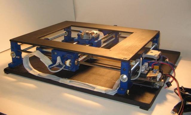
Being able to create PCB’s at home is a milestone in the DIYer’s arsenal. Whether you physically mill or chemically etch boards, it’s a tricky task to perfect. [Charlie & Victor] are working towards a solution to this complicated chore. They call their machine the DiyouPCB. DiyouPCB is an open source PCB etching project consisting of both hardware and software components.
The project is based on using a Blue Ray optical pickup. The pickup was used in its entirety, without any modification, to simplify the build process. In order to use the stock pickup, [Charlie & Victor] had to reverse engineer the communication protocol which also allowed them to take advantage of the auto-focus feature used while reading Blue Ray discs. The frame of the machine is reminiscent of a RepRap, which they used to do preliminary testing and laser tuning. The X and Y axes run on brass bushings and are belt driven by stepper motors which are controlled by an Arduino through a specially designed DiyouPCB Controller Shield.
To start the process a blank PCB board is cut to the final board size. Photoresist Dry-Film is applied to one side of the board before it is put face down on the machine. The PCB design is generated using Cadsoft Eagle PCB Design Software and exported as an HPGL file. The DiyouPCBRun software sends the HPGL information to the custom written Arduino firmware, which in turn controls the stepper motors and optical pickup using the DiyouPCB Controller Shield. The optical pickup’s laser removes the photoresist film from the non-trace areas of the board. The exposed copper is then etched away by means of an acid bath followed by stripping the remaining photoresist film to expose the copper traces. The result is a completed PCB board.
Admittedly, the PCB results are not perfect. The stepper motors are believed to be causing vibration which can be seen in some of the etchings. Axis stiffening and carriage damping reduced the vibration but did not eliminate it. To further combat the vibration issues, [Charlie & Victor] are debating upgrading to servo motors or sacrificing speed by replacing the belts with lead screws.
If you are wondering how you can get one of these machines, it’s easy. [Charlie & Victor] have made all of the necessary project files available on their website for you to download, including the 3D-printable .stl files, software, and controller shield.


This one looked like a cleaner and more simple approach.
http://hackaday.com/2012/08/09/exposing-pcbs-with-a-home-made-laser-printer/
Hi Necromant,
Thanks for the reference. We already knew the laser printer solution you say and it’s a very interesting project but we wanted to do something from scratch: a printer that everybody could build it buying simple comercial components and printing the parts with a 3D printer. Most of the PCB printer projects are based on tier-down and modify inkjet or laser printers. It’s OK but you need a printer to tier it down.
Couldn’t you say the same about requiring a PHR pickup, or any component for that matter? You have even opted to use a discontinued part (not saying they will disappear anytime soon, but it’s a point).
At any rate, nice work with the reverse engineering, very impressive.
When we saw that we could use a blue-ray pickup to sensitize the photoresist we searched on ebay and found that some people (mainly from china) sold the PHR803-T for a resonable price. We bough some of them last year and they still selling units so we think they have the manufacturer stock for spare parts. This pickup is used in the Xbox so probably there is still demand of spare parts. We could use another pickup, probably they would work in a similar way, but this one is very cheap and was available. That was the reason to choose it.
It’s “Blu” Ray, not Blue Ray.
I wonder if one could take advantage of a flat bed scanner and mount the laser in the moving head. (replace the driver electronics etc.) Put a PCB on the glass and let it raster the pattern.
you would need to add the 2nd axis motion to it, flatbed scanners only have single axis movement.
If you used a modified dot-matrix printer head travelling along a flatbed-scanner-style thingamybob, (think ThunderScan here), you might be able to do it?
I would slow that rig down and get it to make good product… then work on speeding it back up for MKII, MKIII, MKIV, MKV…….. the market it. It almost sounds ready now as MK1.
Do you have any idea how many of us are our here that want one rig that will make a good board even if it takes 24 hrs? ONE that will rule for all! One bandwagon we can all jump on?
Those that finally do it will be as those that spent the time in a garage and came up with the APPLE][. I will be knocking at your door along with a very large crowd. 24 hour cycle time is GREAT for now…. aim for 45 minutes in 3 yrs. You will struggle to meet the demand.
Quit thinking about making ONE for yourselves…. we’re out here DROOLING!
They did a nice job documenting their procedure/build.
I would use this machine to etch some urine-relief channels in my toilet seat.
Wow! I was wondering when someone was going to manage this feat, I can’t wait to try this myself now that someone’s worked out the hard part! (The laser)
Where can you get photoresist film at a reasonable price? If Radio Shack really was in the Maker business, they would sell photosensitve boards – I seem to remember they did so long long ago in a galaxy far far away. Must…resist…urge…to…rant
i know Farnell/element14 has them. part nr 141301 and others
I can only imagine what RadioShack would charge for something like that…
Riston seems to be the preferred film to use. I just go for presensitised boards which are easy to get hold of mail order.
Hi JimBon,
You can buy cheap Dry-Film in small quantities at eBay. We bought there the film we used for the printer testing.
@JimBob(or others)
Did you guys(that watched the Superbowl) see the Radio Shack advertisement that claimed “The Radio Shack of the ’80s is gone forever”, or something to that effect. As if they were proud that they were detaching themselves from the days when they actually specialized in hacking and building things as much as they did in offering consumer electronics. Based upon seeing the commercial, it would appear as if they are now going to specialize in consumer electronics, which doesn’t make much sense, since they gave appeared to be moving in that general direction for the last 10-15 years already(excepting the small editions of microcontroller stuff)…
-gave appeared
+appeared
Sorry! I won’t complain about lack of being able to edit posts, though, as IMHO it’s better to let the masses post here without being presented with the threshold of “signing up”… :)
I saw that and wondered if that meant more smart phones, and less components.
The electronic components and support stuff is all I go to RS for. Don’t need phones or that other stuff.
Could it be possible to use EDM instead of a laser?
I guess, but as far as I know, EDM is a much more expensive process, and the EDM methods I can think of are slower for this kind of task.
EDM would be incredibly expensive and take forever.
You would have to use the sinking method and for that you need a graphite tool made and that will be expensive. You cant just move an electrode around, the electrode will wear and cause lots of problems.
ECM would avoid most of those problems. But I wonder if you could get accurate and complete removal of the copper clad.
You would be totally reliant on the flatness of the substrate, which is never good. You would always have copper left over.
No since reinventing the wheel here. Chemical etch works fine. This is just a really complex way of exposing photosensitive boards. There is always laser ablation but you need a very expensive q-switched UV laser.
An old wheel at that.
Many many years ago I worked at a place that produced film masters for bar codes.
It had a little XY CNC stage, driven by a BBC Micro, of all things. You put in a piece of film, and a little laser was moved around to draw the image on the film.
Process film and you’re done.
Of course it got used to make the negatives for photo-exposed PCBs as well. One extra step than what this has, but it’s like 1988(?) all over again…
It looks like this design could relatively easily be converted into a double-sided design by adding another laser head onatopp so that the board is sandwiched between them. Raster scan would probably be more efficient in this case so some parts of the XY table can be optimized, like it’s done in most printers.
Hi Svoski,
Good idea. The actual design was though to print one side of the PCB, then open the printer door, turn arround the PCB, align it with the door window borders and print the other side. This procedure allows better side aligments than tonner transfer which is a nightmare with double-side PCB’s.
You are right also with the idea of a raster printing. We would like to test the printing with Postcrip files instead of HPGL. PS is ideal for raster printing, but we did’nt have time to implementing. Also we unknow if the laser beam will create perfect traces in raster mode.
For toner transfer, I treat it like a single side board. I etch one side
first and use packaging tape to mask the other side. Drill a few
via/holes for alignment when the etching is done. Poke the corresponding
holes on the second print out with mapping pins to line up the hole.
Iron, touch up the holes with marker. Cover the back and etch again.
It takes a bit more work, but I get good alignments with this for double
side boards which are pretty much all I do these days.
Hi Victor. Actually I do double sided toner transfers using a laminator without too much trouble. I print both sides on one piece of paper usually, fold it and glue at the other side so that it makes an envelope. Then I insert copper clad board inside and try not to let it get misaligned when the laminator eats the sandwich. Sometimes it works bettter, sometimes worse, but generally I get it at the first try. I try to pre-compensate for it by making vias larger than they would be on a factory-made board (makes sense doing that anyway for easier drilling). I wish KiCad could make teardrops.
A lot of people here disregard toner transfer as something too primitive and only good for arduinage, but with some skill involved (and with a laminator, just throw away your clothes irons) it’s as reliable and precise as homemade photoresist methods, yet much faster, fewer different chemicals involved too. I used both methods a lot.
Still I find it very interesting that people are developing new methods. And I have quite a few printer parts stashed away waiting for their time ;) I like the both sides at once idea because it allows for imprecise cutting of boards, and still guarrantees alignment. Basically no matter how you throw it in, the sides are going to be perfectly aligned.
Hi svosfki,
Thanks very much for your tips and your support.
We still using toner transfer method because the printer is still not perfect and you know: PCB’s have to be perfect; any defect invalid the complete job.
When I was a kid I used the mark-pen method. It was fine for my electronics skills, but In the last years, I have been using the toner transfer method for double-side PCB’s with very good results. If you are skilled you can obtain good quality jobs. But last year I was preparing one double-side PCB with photoresist for an Arduino shield, trying to align the faces at the dark light of a red bulb and I though: why we still using these indirect methods for make home-made PCB’s? Why any company has developed a direct PCB printer for the hobbits? Then I started to think in the ideal model (we always start our dreams figuring gout what could be the ideal model). Like tekkieneet said: open the door of the printer, deposit the PCB, press a button and PCB ready!!. Then I started to design the 3D model of the printer and built it…The rest of the history is that reality always transform our ideas in something different… that is not ideal :-)
The printer is a DIY printer made with few money, poor means but a lot of illusion. It’s more or less functional. It’s nor perfect and probably toner transfer method is cheaper, faster and we will continue to use it for decades. But we had a lot of fun built it and dreaming that one day we could have one really goooood!. That’s the reason we shared everything with the community, in the hope that people around the world take our designs, improve it and make one day one perfect PCB printer.
You’re doing a great thing and thanks for sharing it with us.
Kudos to them for trying this and getting anywhere with it! I have a lot of respect for those that build these kind of systems. I personally have designed and constructed these types of machines for 3D printing etc and know how much blood and tears go into these.
I just don’t feel that this could ever be any better than the standard photo process. There has been much research into optics and we understand it quite well. At home it is possible to get amazing resolution using transparencies for 3 minutes or so at a time under grow lights. In the industry even more advanced optics techniques are used, but it appears to have scaled well until they had to do some sorcery at the 1-3 atom level….
On top of that, exposure is just one of the problems. If you need the full CNC setup, doesn’t it make sense to mill it out? AFAIK this is just exposing the PCB. It would probably take a bit of time as well to go over the surface. Mounting transparency, and leaving under a UV bulb for <5 minutes is pretty dang fast and convenient. Also it scales well with table/floor space, you don't need a machine capable of your largest batch needs taking up space all the time.
Great hack! I just don't think it is feasible beyond this stage.
Thanks replic8tor,
Yes it was 8 months of hard work with a lot of difficulties and fustration. You can’t see the UV laser painting in a piece of paper and all the testing was made with Dry-Film. It means prepare the PCB, adhere the film, develop the film, etc. It’s very boring.
Milling has lots of issues and you don’t want it for tiny geometry.
Try 0.5mm pitch parts. :P 0.5mm = 20 mils between pads, so you’ll need something like 10/10 or 12/8 track width/spacing. This is easy stuff for photo process (and within reach for toner transfer).
Vibration? Try higher microsteps, this is what microstepping is for, not for a perceived increase of resolution.
Second problem is the design. With the unsupported rods and plastic mounts it probably resonates like a violin. Heavier rods and/or metal rod ends would help. You can also get vibration dampeners to mount on the motor shaft to soak up some of the vibration.
Also try driving both sides of the carriage instead of just from the center. The machine is not tight enough to drive with one point. You could get away with it if you were using rectangular linear bearings, but with round rails and bronze bushings you dont stand a chance.
Thanks macona,
You know very well the problem because your advices are very accurated.
We tried almost everything, even a damper for the motors. I made one with my 3D printer, but it didn’t work. We are using microstepping and also tried with diferent motor models.
Anyway, when designing something always the main problem is what I call “the trade-off”. Inevitably there is a trade-off between diferent components, dimensions, parameters, design criteria…like speed vs quality, or vibration vs cost, or speed vs precission, etc. Believe me, trade-off is always the main problem, not vibration :-)
I never had though that vibrations were so persuasive. It generates at the stepper motors but only at some speed levels. Then, they run through the belts to the pickup.
We practically solved the problem choosing the right speed and making the framework and pickup support more rigid. But the laser beam is 0.1mm of diameter (or less) and any small vibration or resonance move it. So I think we could improve the printer using leadscrews and servos or stepper motors with a gears running faster and a metal framework as you said, but all of this stuff will increase the cost…so, one more time the vile “trade-off”…:-)
check on epoxy-granite at cncforums, it will definitely improve dampening
Some software can skip over frequencies that resonate when driving the steppers. You might look into doing that, though you will need to figure out what the resonant frequency is.
use gears/pulleys/pinions… so it doesnt transfer the vibration to the laser…
A truly awesome and well documented piece of work. That’s obviously taken a fair bit of effort.
I don’t think this will ever better printing on a transparency and exposing – especially for speed – but that’s not what it’s about, is it? It’s about seeing what you can achieve. And these guys have certainly done that.
If anyone does have this amount of time to devote to an improved home PCB production process, I think the holy grail would be to adapt a Xerox wax printer to print onto solid copper clad board. (I know it’s been done on flexible PCBs that can go through the paper feed.) As svofski said, printing both sides at once for perfect alignment would be the nuts. I know I haven’t got the time, but if I did then that’s where I’d focus my efforts.
I guess Peachy printer could do this faster and cheaper.
I guess, but only for very small of a circuit boards. The XY working area is small.
3’x3′ is not very small, but yes, I would like a larger area
” The optical pickup’s laser removes the photoresist film from the non-trace areas of the board.”
No it doesn’t. It exposes the trace areas, the resist on the non exposed areas is removed using the developing solution.
This is just standard negative acting photoresist film, just instead of exposing through an artwork from a wide area UV light, they are exposing traces directly using a focused UV beam.
”The optical pickup’s laser removes the photoresist film from the non-trace areas of the board.”
years and years of people correcting the articles did nothing good to educate the writers here. relax and enjoy the show.
blu-ray, not blue ray.
Actually it says HD-DVD pickup, not even Blu ray, in their website.
The first group of friends that really gets this and turns out a product that works is gonna make a mint. It’s coming soon. Gonna be you? Naww….. Him? Nope! Gonna be someone though! This lil group is just some folks that wanna build one for themselves it seems….. anyone ever get the glimmer that they can get rich?
I don’t see the advantage of this over regular UV exposure using a mask. It’s more expensive to make and a lot slower without producing better results.
Now, put a high power laser there that can vaporize the copper and get a 1 step PCB manufacturing and now we are talking!
I look for a 24 hr cycle time, repeatable, reliable, repetitive process. There is no care which one it is…. what works works.
I’ll pay up to $2500 for one machine that works double sided overnight… push my design into it and get board out, in the home ready for soldering.
How long have we languished? Even you can tell the time is drawing nigh!
Whom will it be that that gets rich?
Yes…. I rant. But honestly, this has been a 20 yr wait so far. I was promised boards… and flying cars….
Your best option is with a CNC router that can mill and drill the holes. An automatic machine which can change the tool by itself will drill and mill one side, then you need to turn it on the other side. I am not aware of any that can turn the pcb on the other side. It will take a long time, make a lot of noise and produce a lot of dirt.
The machine presented here doesn’t bring the process of uv exposure closer to a one step. Instead of printing on a transparency, putting it on a board and exposing(5 min job) you put the pcb inside and print it (looong time). You then have to do with all the same steps on both: develop, wash, etch, wash, drill holes. So it doesn’t make much sense….
Here ya go: http://youtu.be/mzmjGz0_joM?t=28s
I am absolutely aware of that, i’ve seen it quite a few years ago. But there is no diy version, is it?
I remember going through their documentation to find out the laser power…but with no success.
Now they have machines that can also drill the holes, so it is really a one click to pcb solution…i wonder how much it costs…
They have 500-1000W Q-switched laser, cost is around 100k$.
It seems they have not identified all pickup pins (quite a lot are not connected in the pickup driver schematic). Among the unused pins, they talk about a “RF signal” pins. Since they can already turn laser on and off and modulate its power, what this “RF signal” can be used for? And what can be the other unused pins? Any ideas?
Gerald,
Yes, it was difficult to figure out just the few pins we needed so we din’t continue researching the rest.
The RF are documented in some CD/DVD manuals. Are two pins used by the CD/DVD/Blue-ray reader to obtain the modulated signal of the music recorded on the disk surface. We think we found those pins because we obtain a signal with the oscilloscope but we didn’t need them for the printer.
To me, this is the most interesting part. I think that by driving the focus mechanism with a reasonably-fast signal, you might be able to fine-tune the focus as you move, without overly exposing the film to an out-of-focus beam.
This would compensate for imperfect flatness of the PCB, which is where most other printers and engravers have trouble. Even just a fraction of a millimeter travel could improve quality across the whole board surface. Someone will tackle this problem, sooner or later. :)
Documenting the pinout of this module, and contributing to DIY knowledge about this mechanism, is super cool. Thank you! Both for the hard work, and for the detailed writeup.
Cool. I bet a lot of the problems they were having could be fixed by using ball screws instead of belts. A bit more costly and the printer may not be as fast, but they would get more precise motion which is needed for ultra fine PCBs.
Currently I’m using a desktop CNC with V-bit to mill my own PCBs and I have no problems with accuracy due to the ball screws used in my machine, but I’m having trouble with the V-bit itself since it cant cut a channel less than about 10mils due to runout and PCB thickness tolerances/warping.
This means that I struggle with really fine pitch components so I have been thinking of trying to mount a laser to the CNC to use it to expose a PCB instead.
Nice work!
1st of all .. my respect .. a lot of pioneer work ! I want to build a part of it (Part, because i owe a CNC milling machine already which can do the XYaxis movements). Are you willing to support me, as i made a full page of notes with questions already. The material which is free for download gives an idea, but is not enough/complete to build a machine.
My motivation: I’m a radio amateur building radio equipment in the 76 -145 Ghz area. If you want to produce very small structures on a thin PCB w/ teflon substrate milling will fail as i encountered painfully. Your design is based on a mechanic that does the XY movements like a CNC milling machine. The Laser part is solved by a ready to use module, with the very elegant feature of auto-focus. That is a great basis for a precise exposure, as you never get completely plain PCB boards.
So again .. are you willing to stand a lot of detailed questions ?
:-) OE3WHU Wolfgang
Hi! :)
What is Blu-ray head used?
Drive model tell?
The pickup model is Toshiba PHR803-T
You will find complete info at our web page: http://www.diyouware.com