Making your own printed circuit boards – as useful as it is – is a pain. Using the very popular toner transfer method requires a dozen steps that have to go perfectly the first time, and milling boards on a CNC machine creates a lot of mess. The most industrious hackers are able to bodge up a direct-to-board printer from an old inkjet printer, but these builds are usually a little kludgy. [Tixiv]’s LaserExposer board printer is one of the first builds we’ve seen that does away with all the negatives of the other techniques of PCB manufacturing and turns making your own boards into a very, very simple process.
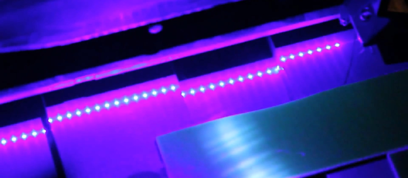
The LaserExposer uses photosensitive copper board, like many of the other PCB printers we’ve seen. Instead of printing out the board artwork to a transparency or mask, [Tixiv] used a 1 Watt 445nm blue laser with a hexagonal mirror to directly expose the artwork onto the board, line by line.
The entire device is built around an old flatbed scanner that slowly crawls over the PCB, exposing the traces of copper to be etched away. This required reverse engineering the mirror motor control board from an 90s-era laser printer and building a circuit to precisely control the timing of the laser. [Tixiv] eventually got everything working and after etching had some of the most professional looking home-brew boards we’ve ever seen.
[Tixiv] put up a demo video of his build (after the break, German audio, YouTube has captions…). Anyone have an old flatbed scanner lying around?
[youtube=http://www.youtube.com/watch?v=fi4P-Bwc6g8&w=470]






I think the diode is 450nm not 45nm
you mean 405nm. its a blue ray laser diode.
sorry, shame on me. its from a beamer, so its 445nm.
sed s/Anders/Tixiv/g
It not my project. I only found it on youtube and liked to share it. Tixiv is by the wiki-page the author of this fine project.
“Using the very popular toner transfer method requires a dozen steps that have to go perfectly the first time, ”
Only if you are doing it wrong. Get the transfer paper MADE for this and it’s super easy. Dozen steps? how about 4.
Load special paper in printer, print, iron on, peel off…. All done unless you count etching as a step, then it’s 5.
http://www.dipmicro.com/store/PNPB
If you are too poor to afford that stuff, you should choose a different hobby.
That sounds like a time consuming pain in the ass that a clever, industrious hacker would just build a device to do for them.
If you can’t see the value in that than you should choose a different hobby.
Of all the DIY methods, Toner transfer pretty much wins hands-down.
Double-sided, vias, soldermask etc are problems, but all the other methods fail to varying degrees there too.
One interesting project is to hack a laser printer to print directly onto the PCB – skipping the transfer part.
This project is similar – it skips the ‘make a negative’ bit.
Best. Response. Ever.
No captions on the video here….
I don’t see any eye protection anywhere…
But cool hexagonal mechanism.
Wasn’t he the same guy who did the Hacking the DTV-64 talk? Very interesing.
Anyway, this seems to be a re-invention of the wheel. Photo resist board is designed to be exposed to UV light. What is the problem with using a UV light box?
You missed the point. Traditionally, to use the UV method, you would print out your design on velum, line up the velum and the board, and then expose in a light box. This project avoids printing the velum, you are directly printing the board.
Yup, great for one-off prototypes.
I’ll watch the video when I’m not at work, but it sounds like a nice project. (Personally I mill mine which lets me drill and cut out custom shapes on the same machine that are perfectly aligned.)
What’s really missing from all home PCB manufacturing is a decent solder mask. If anyone knows of a good way then let me know.
There’s some tubes of UV curable solder mask paint sold on Ebay. Apply a fairly uniform layer, let dry, expose, and remove the uncured paint with the specified solvent. I have some, but haven’t tried it yet.
Better would be the film real board manufacturers use, which can be laminated on for a perfectly uniform layer. I’ve searched, and can only find it in huge (and expensive) rolls. If anyone knows where to get just a few sheets, I’d be interested.
I decided to look again for the film, and it seems that someone is finally selling it in small quantities. Search Ebay for “dry film solder mask”.
Great find. Thanks. Of course now I’ll have to get a laminator and UV source, so might end up etching rather than milling!
Instructable by the eBay seller about using it here:
http://www.instructables.com/id/Dry-Film-Solder-Mask/
I have seen ‘Liquid tin’ on ineternet, seems to be easy and have nice results
That isn’t a solder mask. The solder mask covers everything but the areas where you want solder to wet.
This is what baffles me about HaD. One day you are talking about printing circuit boards like making a ham sandwich and the next day it is this Sisyphean task. Similar with the acronyms. Oh well. Interesting video.
Very nice .. photo-lithography without messing around making the mask. I would imagine this method can generate a very fine pitch, limited only by the diameter of the beam?
I’m a fan. I’ve got an old scanner that is so slow it hurts. Good to see a use for it.
This is the best hack for this year. Exactly what I need. And it even works in high quality and not the shitty sort-of-works-kind which people usually get when making pcbs. Awesome!
Great hack. Sure, some may consider it overkill. But the quality and the repeatability of something like this are undeniable.
Very nice project..
I can see getting a pico projector from microvision and just use their blue laser to do the exposer . One inputs the video and set the distance to get the correct spatial dimensions and then expose for couple of minutes and then into the developer and etch. It would eliminate the scanning motor and flat bed and custom software.. and maybe only three minutes to make an exposed board.
I had this same idea a couple years ago when ask.hackaday.com was still around and everyone said it was stupid.
If it’s stupid but it works, it’s not stupid. (Murphy’s second law of combat)
Hi Brook_Lee
It really is not stupid if you think about it. MicroVision uses three lasers to generate their color video. Blue is the 450 nm diode laser and they got a green diode laser which is like 522nm Im not sure who is providing that one. I do not think its a DPSS green laser as its to expensive to modulate (You can’t modulate the pump laser).Then a Red diode laser in the 658 nm range. The beauty of the laser projector is their no front focusing element. It’s just geometrics to get the right spatial dimensions and the right energy density for exposer which can be adjusted by exposer time. The laser retains it small beam size and is scanned just like this project in both the X & Y axis.
One could also use a DLP and filtered lamp to get the UV/Blue light just like in 3D printers that use photo polymers. This approch may even be easier as you can get the DLP on ebay at a pretty good price….
using the projector would be limited by the projectors resolution, which would probably be very limiting when making PCBs.
I see it’s a scanning mirror. if driven slowly, it might have very high accuracy, and would be great for pcbs.
Treat it like a stepper in the Fabs. (or an old darkroom enlarger for film in reverse.) Expose, then move over. Any resolution you need, down to the current limit. All you need are the right optics.
Of course, the mechanics of it gets a lot more complicated than on a scan line implementation like this one. Tixiv’s design is only limited by the spot size and focus/collimation of the laser and the minimum step of the board. I don’t think his optics are anywhere near close to diffraction limited yet, plenty of room for improvement. Just look at the resolutions capable on professional scan line drum scanners.
Silk screening, parallel process capable of multiple boards at once. Limited by screen LPI and viscosity of the ink used as the resist. FAST
Contact printing, parallel process, limited by printer size and resolution of the negative. FAST
Photolitho projection, fast, expensive masks, expensive optics, expensive mechanics. Features down to, (what is it now?) 22nm/ 18nm?
DLP projection idea, feature size??? speed is limited by the resolution needed, multiple exposures needed to compete with contact printing, but theoretically capable of smaller features, similar problems as standard photo-lithography used in the industry.
Scan line laser, limited by laser spot size, Transverse mode and diffraction of the wavelength used. Should be capable of some quite small features. Slow, limited by exposure time needed and serial output.
I think that sums it up, except for electron beam litho, which should be similar to the scan line laser method with smaller feature sizes.
I am now disappointed with my laser printer.
One could also use a dlp projector and simply project the image as blue channel / put in an UV LED. That would be simplest, but the resolution would be like 1024×768
I have been planning to make that for a few months now, have a cheap DLP projector ready to go. You can also remove the DLP’s color wheel and then project on all channels (4x exposure over blue channel)
And although limited resolution, you can always enlarge the image area for bigger boards.
I was also thinking of similar project. But you could however expose the pcb in small pieces to get big resolution. That would of course requice XY-table and precise alignment.
Ok.. what’s the magic for bringing up the captions?
OOh. My boss just (a few months ago) offered me a large format scsi scanner he never used. I declined because I had no use for it at the time. My wife would not let me bring another “computer thing” home (unless I had a use for it?). Now maybe I will re-think my decision. I actually had an idea similar to this using a led laser converted with an UV diode. The idea seemed a little slow at the time (drawing like a CNC machine) and I did not have the resources to make one (I have no real need for such a luxury). I guess I should start sourcing the other parts and see if I can do it.
Ahhhh! Just when you think you have an original idea someone on the internet beats ya to it. I was just started working on a very very similar project last week. I also was planning to start with a scanner as the base chassis of the device. I am fascinated by his use of the orthogonal mirror set up though. Good execution! I am glad that it works as I now know that when I finish mine it won’t end up being a waste of time.
This is incredibly cool just because it’s such an awesome hack — a homebuilt laser printer, even though made from another laser printer. But I wouldn’t really say that the result is dramatically better or easier than toner transfer. Indeed, as others have pointed out, if it’s a painful and unreliable process for you, you’re doing it wrong and you probably don’t have enough skills to make a homemade laser printer :)
I like the idea, seen it done before. but… how do you manage aligning double sided boards?
On another hand, anyone knows what power the laser needs to be to directly vaporize the copper? like the guys at lpkf do?
1.27 jigawatts
for cutting pcb-s we used 200W CO2 laser with a 2kW RF power supply, but it would only cut through laminate, not copper, copper reflects infrared too well, you would need UV laser
Or, you could use near infrared (NIR) lasers instead.
For laser-cutting or -etching metals, ~1000nm light works well (as opposed to ~10000nm light that CO2 lasers emit), as from an ytterbium fiber laser or a Nd:YAG laser. Since Epilog seems so popular, I’ll mention their (10 to 50 watt) FiberMark lasers, which are for _marking_ metal, only. Multi-kilowatt NIR lasers are used to cut through some sheet metal.
~1000nm lasers aren’t as generally useful for laser cutting and etching as ~10000nm lasers are, but they do have some relatively specialized uses. For instance, you can’t effectively cut wood or acrylic with the longer wavelength laser, since wood, plastics and most other non-metallic materials won’t effectively absorb the energy such light. Metals generally will, though.
To my knowledge, this means that using such a NIR laser to directly raster- or vector-etch the copper off a CCB to make would work rather well, since the nonmetallic substrate would significantly affected if the laser is set to a somewhat higher power setting than necessary to simply vaporize the (usually 35 micron thick) layer of copper.
alternatly take a plotter, flatbed scanner, and laser assembly, replace the laser printers constant rpm head with a stepper, and you have a laser plotter?
I ownder if you could get a laserprinter to feed a table to make a raster based machine….
hmmm
Awesome build.Great work on the software and the parts used. But indeed for it to be handy you would need to skip the chemical baths part (otherwise it’s indeed not much different from a toner transfer…). You need a stronger laser that directly burns out the traces without using all those chemicals afterwards (cfr like lasercutter). But this should be great with a more powerfull laser like mentioned the LPKF pcb printers. Until then a cnc with vacume is easier to use (it’s fully automatic: stick in board, get finished pcb when machine is done… Not stick in board, then use loads of dangerous unhealthy chemicals in 2 steps and well ventilated area with gloves + wait for just the right time to pull it out.
PCB routers have to be surprisingly precise, particularily in the z-axis. See the “mechanical trace isolation” section of http://www.precisebits.com/tutorials/pcb_mech_etch.htm.
The chemicals used for chemical etching don’t have to be that bad, actually. For developing positive photoresist after exposure, sodium metasilicate is superior to (and also safer than) sodium hydroxide. The safest, but also slowest, etchant available is white vinegar + hydrogen peroxide + non-iodized (pickling) salt.
i have a flat bed scanner and an oki printer ( the one with led arrays ), lying in a closet. i had the idea in mind. i didn’t find any schematic for the printer.
i like this idea
a real photoplotter, and amazing how simple it is, this is exactly how pcb-s are exposed in fab houses. focusing problem on the edges/center can be fixed with a magnetically moved lens like in cd-rom-s, this should work right? now if only someone figured out the electroless process to be made simply at home, it would really be possible to make reasonable quality pcbs at home. so far making pcb-s at home really isnt worth it, quality is too crap, vias are not metallized, nobody uses soldermask for home made pcb-s. if someone figured out electroless process only thing missing would be surface finish, but that shouldnt be too hard i think, atleast for tin finish, Ni/Au would probably be too difficult
I like the Tixiv’s method, it’s great, but to be able to produce 2 layer PCB with it, one needs to align & glue 2x single L. PCBs. Or Tixiv to produce a ‘stereo’ version – with synchronous 2-side exposure. Although it’s hi-tech, and best method for exposure, it doesn’t look easily reproducible.