Everyone has their favorite process for PCB fabrication, as long as you’re a happy hacker I don’t think it really matters. But in this post I thought it might be interesting to describe my personal process, and some of the options available.
Making your own at home

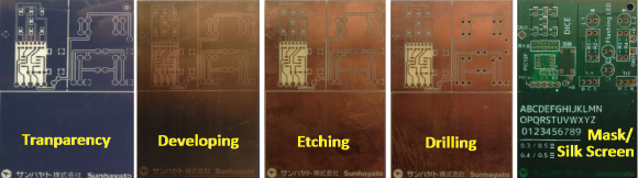
Etching is the classic PCB fabrication option for the home hacker. It’s been many, many years since I etched a PCBs but it can produce interesting results. Some people don’t like it, and I’d personally tend to avoid it as a messy and finicky process. But, if you only need 1 or 2 layer boards with large features (through-hole components are best of course) it can be a viable option. In some cases, I think etched boards look awesome and are a great fit. One example is the skull etching shown to the right. The oxidation and discoloration of the boards adds to the design aesthetic in this case.
For those with a bigger budget a professional milling machine might be a viable choice. I’ve used an Accurate CNC in the past (LPKF and others make mills too), but this is an expensive option (no online pricing, but if $10,000 USD is a lot for you don’t bother). The accurate mill is pretty awesome, it can be fitted with a vacuum bed, automatic tool changer and vision system for alignment. The mill can produce high quality two layer boards with all the holes and vias drilled out. The final step of filling the vias is however manual, but compared to etched boards the results are pretty professional (the mill itself uses milled PCBs!). They claim a 0.1mm (4 mil) track size, I’ve never tried tracks this small but surface mount components were not a problem.
While a fun toy, it’s worth considering if you really need a PCB mill. The only case where they’re really valuable is if you want to be able to iterate over a design with less than a days turn around. This can be useful in RF or low noise designs where you might want to experiment with different layouts, but for other projects the price of a good mill can pay for quick turn around (1 or 2 days from order submission to delivery) on a lot of boards.
Commercial Fabrication
Years ago commercial fabrication used to be a very expensive and finicky process. For the most part you’d need to order a full panel putting the service outside of most hobbyists reach. Generating gerbers and drill files to the fabs specification could also be a process fraught with complication.
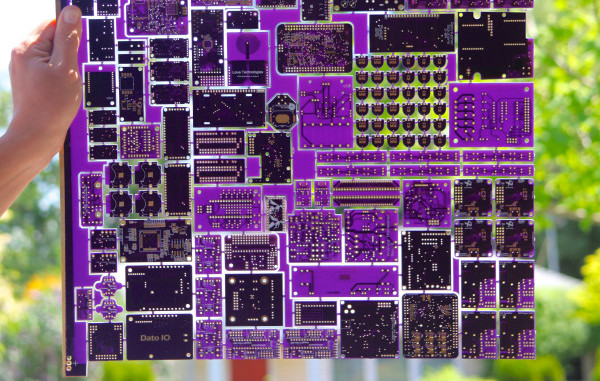
These days services that aggregate designs onto a single panel and break them out for distribution are common. For my work I mostly stick with OSHPark and SeeedStudio whose services complement each other well. I’ve also used Itead and found them compatible with Seeed (with the added benefit that they supply free boards for open projects).
Using OSHPark gives me the warm fuzzies. A child of the hacker community, born out of DorkbotPDX, all OSHPark’s boards are fabbed in the US (check out the great amphour interview for more details). Their services are limited to either 2 or 4 layer boards (always in purple, and always coated with gold (ENIG)), in 6×6 (6 mil traces with 6 mil spacing) or 5×5. I rarely attempt BGA boards so the 2 layer service works out great for me. OSHPark’s minimum order is 3 boards, which is perfect for prototyping. The gold plating also provides a nice finish, which both protects the board from oxidation and provides a nice surface to solder to. The main reason I use OSHPark however is that they’re cheap for small boards and have a relatively fast turn around (I recently purchased 3 tiny 20x15mm boards for $2.40 including shipping which was unbeatable). From OSHPark in the US to the UK my boards take about 2 weeks to arrive. They’ve also automatically upgrade boards to their super-swift service for free when there’s spare capacity. Their service is pretty slick, and provides a rendering of the gerbers prior to ordering as a final check which comes in very handy.
Seeed on the other hand are much cheaper for larger size boards and volume orders. They also provide more color and finishing options. The cheapest option at Seeed is green PCBs with HASL finish (hot air solder leveling). From Seeed, my boards usually take about a month to arrive (there are a few delivery options, but in my experience this is about as fast as it gets and faster shipping services often make using Seeed less attractive).
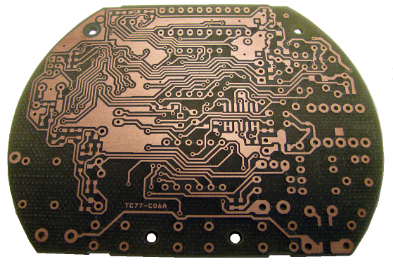
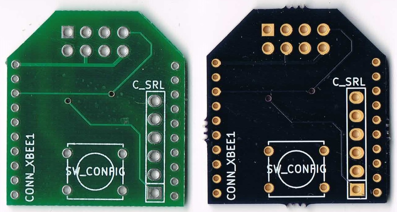
The image to the right shows a couple of very simple boards I had manufactured at both OSHPark and Seeed. I’ve never had a fabrication issues with boards from either service (though I prefer the ENIG finish).
Partly due to the limitations imposed by using commercial fabs I pipeline my projects. I send projects out to fab early in the design process and then switch to another design. When the board comes back I bring it up, bodge as required, and iterate over the layout. This works well with a two-week turn around, so I mostly use OSHPark while prototyping.
My boards also tend to be quite small (Arduino shield size or a little bigger). With small boards like this OSHPark is usually on-par or cheaper than ordering from Seeed (whose minimum quantity is 10 boards). With boards of about 100x100mm or larger I consider Seeed as they become significantly cheaper.
As a hobbyist I also rarely need huge numbers of boards, but for workshops when I need 10 or 20 boards I order from Seeed based on the final iteration of my prototypes. This is not only much cheaper than OSHPark, but I can get boards in a variety of colors to make workshops more interesting too.
This post has described some of the available options and my personal process. I hope it’s been interesting, but I’d love to hear about your favorite fabrication techniques, services and experiences both good and bad too. Please comment below!