Here’s a PCB fabrication process that makes us envious. It’s pretty darn close to fab-house quality at home. [Cpirius] is using a CNC mill and through hole plating technique to produce his double-sided circuit boards.
The video embedded after the break shows one board from start to finish. It begins with the mill drilling holes through some double-sided copper clad stock. Once the millings have been cleaned off the holes are coated with a mixture of waterproof ink and carbon. This prepares them for plating by making the holes themselves conductive. The board is then run through an electroplating process based on this guide.
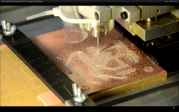
Possibly the most interesting part of the process starts 52 seconds into the clip. The mill uses a conductive probe to generate a height map of the entire board. This allows it to vary the routing depth for perfectly cut isolation traces. That final routing process is pictured above.
[via Dangerous Prototypes]


Very cool! Nice Work! But I gave up watching the video 30 seconds in… It looks like it could use some G code efficiency improvements. It makes a lot of unnecessary moves.
@ 8:15 he says “g-code needs some efficiency improvements”
Hehe, yes, the gcode inefficiency is definitely a problem. I have plans to rework the software process of converting gerber files to gcode with my own code, but I have no idea when I’ll be able to complete that. For now I just do other things while it’s cutting, but I would like to find some intermediate way to optimize the gcode.
Hi Cpirius! How did you build that? It’s simply amazing.
Looks neat, but I would be concerned that is the trace was made too thin, it might lift off the board during production.
The coppers adhesion to the FR4 board material is surprisingly strong. I haven’t had any problem with the copper lifting off, even with very small traces and component pads.
I haven’t done any minimum trace tests yet, but I can make 6 mil traces without problems.
This, on a reprap…
I wondered how indexed the board when he pulled it off to through hole plate, and to route the backside.
I would guess it’s by using the corner holes. They’re drilled through into the spoilboard so just pop some suitable diameter pins in and you’re sorted.
I’ve done some isolation routing myself and must sort out some height mapping. First I’ll try vacuum hold down to see if that gets the PCB flat enough to not need it.
Pegs in the corner holes is my plan, you hit that right on ;)
I don’t have it setup quite yet though. I’m planning to make a jig to hold the pins in different slots for whatever size board I need. I’ll put up a video of that after I build it.
At the moment I’m lining it up manually :( I use Mach3 to put the bit point were the hole should be and move the board to that location. I do that a few times with different holes on the edges of the board until the orientation is accurate.
Probably nice work, but without editing, the video is a major snooze fest.
At least it isn’t bogged down with some stupid soundtrack.
And I’m pretty sure I’ll be using the “Activate the holes” saying – just because it’s cool.
Bozo, that’s what fast forward is about – it’s a cool new feature in video players
@Mike – when your viewer has to fast forward – that’s an indication that editing is needed. It’s not a hard concept to understand. Feel free to post what part of that idea is beyond your comprehension and maybe someone here can dumb it down enough for you to understand.
Wonder Twin Hole Powers… ACTIVATE!
The video did get longer than I really wanted it to be, but I wanted viewers to be able to watch more of the cutting process if they wanted to, and skip it if they didn’t. Now that I think about it though that would have been easier if I had made a condensed production steps video in the beginning and added extra cutting video after, or in a second video. I’ll do that next time ;)
Wow this is great.
I can see how the process is much easier with isolation milling rather than etching traces, but I always thought that isolation milling is a really cool way to make a one-off board prototype anyway so this works for me. It’s a good way to make one board to try your design and verify it’s right before sending it off to have multiple copies made if nothing else. Isn’t there always at least a couple errors or tweaks with a board design you would have liked to find before you ever ordered that alpha batch?
I have looked at the think & tinker conductive ink but the price is very high and not worth it unless you do a fair bit of this kind of thing, considering the shelf life and all.
So to me the eureka items are the dirt-cheap conductive ink and the probing routine for compensating for board height, which is tricky and not reliable with my mechanical methods for trying to just make things flat. The probing looks like it makes it dead easy !
Clever info to glean from your site. I for one am tickled that you have shouted it from the rooftops. I will definitely be trying your methods myself.
“It’s a good way to make one board to try your design” I have never ever had to do this. my first board is from BatchPCB with about 10 of it’s identical twins. You can verify a pcb is 100% without ever etching one. and changes are easily done with wire wrap wire and an exacto knife just like they do in the big manufacturing houses.
Thanks! I’m glad you liked it :)
I’ve found that fast prototypes can be very useful. I do a lot of fast turn around designs, usually involving chips with footprints that really need a board (QFN, DFN, etc), and it’s very helpful to be able to prove different designs, or try multiple variants quickly without having to wait for a boardhouse or pay high expedited production fees.
I had an idea… how about routing pcb traces into a clean non plated board and then squeegee conductive ink into the traces? Well ok… maybe not fantastically productive, but different :)
I’ve done what your suggesting, it works using fiberglass sheet, predrilled, and than activated and electroplated but it takes for ever and after etching the traces your still left with the conductive ink shorting everything out and its a pain to fully remove. Although a mill would probably remove the ink as well so may work better in that case. 2 cents
The conductive ink I’ve tried is pretty high resistance. I tried it to fill in 3 holes from top to bottom layers on a sample board and it was about 3Ω resistance. I’m sure more holes would lower this but it was kind of disappointing.
What kind of milling heads is he using? I’ve tried a number of heads but I kept running into the issue of strands of copper forming from the cut.
Milling heads as in the type of bits I’m using? I use 60 degree tungsten carbide engraving bits. They are cheap and effective. I’m not sure exactly what you mean by “strands of copper forming from the cut”, but it doesn’t sound like anything I’ve seen happen to me.
So he did some cool PCB routing…Where’s the information on it?! It ain’t anything nearing a hack if it’s just some guy showing off.
Sorry there’s not a ton of information. This is still very much a work in progress for me and I’m working on improving the process. I’d be happy to make a complete write up with all the details ones I have it figured out, but I can’t give any guarantees on how long that will take. For now, there are some details in the video description about most of the software/procedures that I used.
I don’t see any details on the make-up of the conductive ink. What sort of “waterproof ink”? What proportions of ink and carbon? This has been the stopping-point for me doing my own PCBs.
higher speed servo motors ensure clean traces without lifting from the board. 24000rpm is good.