A Vacuum Battery Made For Looks And Learning

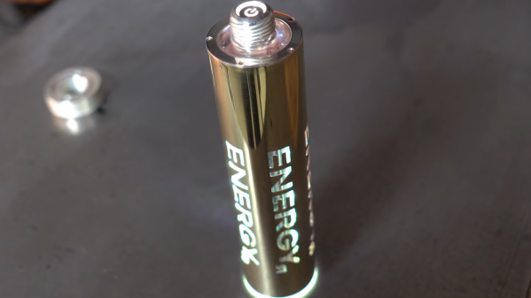
Looks and RGB LEDs are usually not a priority in tool batteries, but [Oleg Pevtsov] decided the battery for his DIY vacuum cleaner needed to be different. In the process, he learned some lessons in chemical etching, plating, machining, casting, and electronics. See the video after the break for the build compilation.

The core of the battery is just five 18650 cells in a 3D-printed holder with a BMS, but the real magic is in the external components. The outer body is a brass tube with the logo etched through the 0.6 mm wall. Getting the etching right took a few tries and a lot of frustration, but he eventually found success with a solution of sulfuric acid and nitric acid in a magnetically stirred container. For etch resist he sprayed lacquer on the outside and filled the inside with silicone. The inside was then coated with clear epoxy by allowing it to cure while spinning. The final touches were nickel plating, then gold plating, and a high polish.

The silver-plated connector on one end consists of a machined copper tip and ring, epoxied together for isolation. The tip has a multi-start external thread, allowing the female side of the connector to securely connect with a single twist. A set of RGB LEDs were added to the core to light up the battery from the inside. We have to hope the vacuum this is supposed to attach to is equally impressive.

This being Hackaday, we see a lot of custom power banks for all the custom electronics. These range from a small power bank for on-the-go soldering to a heavy metal beast with a built-in inverter.

Continue reading “A Vacuum Battery Made For Looks And Learning”

Printing, Plating, And Baking Makes DIY Microlattices Possible

To be honest, we originally considered throwing [Zachary Tong]’s experiments with ultralight metallic microlattices into the “Fail of the Week” bucket. But after watching the video below for a second time, it’s just not fair to call this a fail, so maybe we’ll come up with a new category — “Qualified Success of the Week”, perhaps?

[Zachary]’s foray into the strange world of microlattices began when he happened upon a 2011 paper on the subject in Science. By using a special photocurable resin, the researchers were able to use light shining through a mask with fine holes to create a plastic lattice, which was then plated with nickel using the electroless process, similar to the first half of the electroless nickel immersion gold (ENIG) process used for PCBs. After removing the resin with a concentrated base solution, the resulting microlattice is strong, stiff, and incredibly light.

Lacking access to the advanced materials and methods originally used, [Zachary] did the best he could with what he had. An SLA printer with off-the-shelf resin was used to print the skeleton using the same algorithms used in the original paper. Those actually turned out pretty decent, but rather than electroless plating, he had to go with standard electroplating after a coat of graphite paint. The plated skeletons looked great — until he tried to dissolve the resin. When chemical approaches failed, into the oven went the plated prints. Sadly, it turns out that the polymers in the resin expand when heated, which blew the plating apart. A skeleton in PLA printed on an FDM printer fared little better; when heated to drive out the plastic, it became clear that the tortuous interior of the lattice didn’t plate very well.

From aerogels to graphene, we love these DIY explorations of new and exotic materials, so hats off to [Zachary] for giving it a try in the first place.

Continue reading “Printing, Plating, And Baking Makes DIY Microlattices Possible”

PCB Finishes Hack Chat

Join us on Wednesday, March 11 at noon Pacific for the PCB Finishes Hack Chat with Mark Hughes and Elijah Gracia!

There’s no way to overestimate the degree to which the invention of the printed circuit board revolutionized electronics. What was once the work of craftspeople weaving circuits together with discrete components, terminal strips, and wiring harnesses could now be accomplished with dedicated machines, making circuit construction an almost human-free process. And it was all made possible by figuring out how to make copper foil stick to a flat board, and how to remove some of it while leaving the rest behind.

​Once those traces are formed, however, there’s more work to be done. Bare copper is famously reactive stuff, and oxides soon form that will make the traces difficult to solder later. There are hundreds of different ways to prevent this, and PCB surface finishing has become almost an art form itself. Depending on the requirements for the circuit, traces can be coated with tin, lead, gold, nickel, or any combination of the above, using processes ranging from electroplating to immersion in chemical baths. And the traces aren’t the only finishes; solder resist and silkscreening are both important to the usability and durability of the finished board.

For this Hack Chat, we’ll be talking to Elijah Gracia and Mark Hughes from Royal Circuit Solutions. They’re both intimately familiar with the full range of PCB coatings and treatments, and they’ll help us make sense of the alphabet soup​: HASL, OSP, ENIG, IAg, LPI, and the rest. We’ll learn what the different finishes do, which to choose under what circumstances, and perhaps even learn a bit about how to make our homebrew boards look a little more professional and perform a bit better.

join-hack-chatOur Hack Chats are live community events in the Hackaday.io Hack Chat group messaging. This week we’ll be sitting down on Wednesday, March 11 at 12:00 PM Pacific time. If time zones have got you down, we have a handy time zone converter.

Click that speech bubble to the right, and you’ll be taken directly to the Hack Chat group on Hackaday.io. You don’t have to wait until Wednesday; join whenever you want and you can see what the community is talking about.

The Clickspring Playing Card Press Is A Work Of Art

We have no idea what a playing card press is, nor do we care. All we know is that after watching [Chris] from Clickspring make his playing card press, we want it.

Digging a little deeper, [Chris] offered to make this card press for [Chris Ramsay], a magician who specializes in cardistry, or the art of illusions with cards. The feel of playing cards is crucial to performing with them, and a card press keeps a deck of cards in shape. Not a commonly available device, [Clickspring Chris] designed one in an elaborate style that brought in elements from [Chris Ramsay]’s logo.

Like all Clickspring videos, this one is a joy to watch, but in a departure, there’s no narration — just 30 minutes of precision machining and metal finishing. [Chris] has gotten into metal engraving in a big way, and used his skills to add details to everything from the stylized acorn at the top to the intricate press plate, all of which was done freehand. And those snakes! Made from brass rod and bent into shape by hand, they wrap around the side supports to form [Chris Ramsay]’s logo. All the brass ended up gold plated, while all the screws ended up with a heat-blued finish. Settle in and enjoy the video below.

It’s been a while since the Clickspring skeleton clock was finished, in which time [Chris] has been working on a reproduction of the Antikythera mechanism. His video output slowed considerably, though, when he made a new finding about the mechanism, an observation worthy of writing up as a scholarly paper. We can’t begrudge him the time needed to pursue that, and we’re glad he found time for this project too.

Continue reading “The Clickspring Playing Card Press Is A Work Of Art”

Chemistry And Lasers Turn Any Plastic Surface Into A PCB

On the face of it, PCB production seems to pretty much have been reduced to practice. Hobbyists have been etching their own boards forever, and the custom PCB fabrication market is rich with vendors whose capabilities span the gamut from dead simple one-side through-hole boards to the finest pitch multilayer SMD boards imaginable.

So why on Earth would we need yet another way to make PCBs? Because as [Ben Krasnow] points out, the ability to turn almost any plastic surface into a PCB can be really handy, and is not necessarily something the fab houses handle right now. The video below shows how [Ben] came up with his method, which went down a non-obvious path that was part chemistry experiment, part materials science. The basic idea is to use electroless copper plating, a method of depositing copper onto a substrate without using electrolysis.

This allows non-conductive substrates — [Ben] used small parts printed with a Formlabs SLA printer — to be plated with enough copper to form solderable traces. The chemistry involved in this is not trivial; there are catalysts and surfactants and saturated solutions of copper sulfate to manage. And even once he dialed that in, he had to figure out how to make traces and vias with a laser cutter. It was eventually successful, but it took a lot of work. Check out the video below to see how he got there, and where he plans to go next.

You’ve got to hand it to [Ben]; when he decides to explore something, he goes all in. We appreciate his dedication, whether he’s using candles to explore magnetohydrodynamics or making plasma with a high-speed jet of water.

Continue reading “Chemistry And Lasers Turn Any Plastic Surface Into A PCB”

Through Hole Plating And Milling At Home

Here’s a PCB fabrication process that makes us envious. It’s pretty darn close to fab-house quality at home. [Cpirius] is using a CNC mill and through hole plating technique to produce his double-sided circuit boards.

The video embedded after the break shows one board from start to finish. It begins with the mill drilling holes through some double-sided copper clad stock. Once the millings have been cleaned off the holes are coated with a mixture of waterproof ink and carbon. This prepares them for plating by making the holes themselves conductive. The board is then run through an electroplating process based on this guide.

Possibly the most interesting part of the process starts 52 seconds into the clip. The mill uses a conductive probe to generate a height map of the entire board. This allows it to vary the routing depth for perfectly cut isolation traces. That final routing process is pictured above.

Continue reading “Through Hole Plating And Milling At Home”