Researchers at the University of Tokyo, Georgia Tech and a team from Microsoft Research have developed a low-cost method of printing circuits using an ordinary inkjet printer using a technique called Instant Inkjet Circuits.
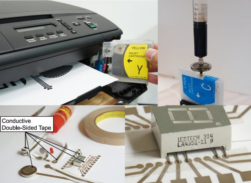
The hack is quite literally as simple as injecting a refillable printer cartridge with a commercially available Silver Nano-particle Ink. This allows the printing of circuits onto many different flexible substrates including paper, transparent film, or basically anything you can fit in the printer. Typically if the medium is designed for printing it will work. Some exceptions to this include canvas cloth, magnetic sheets, and transfer sheets.
The researchers chose a Brother inkjet printer because they typically have nozzles that eject higher volumes of ink than other printers. The exact model they used was the Brother DCP-J140w. To maximize ink deposition, all cartridges are filled with the ink, and printed using photo mode where the C M and Y cartridges are simultaneously used to create black. No special software is required to print.
The full article is well worth the read and shows many examples of the different applications this could be used for — including instant prototyping using nothing but scotch tape.
If anyone can source some of this ink and try it out we would love to hear from you! Those that can’t may want to give the old inkjet/laser toner etch resist trick a try.
[via Power Electronics]


They probably also chose a Brother printer because, in my experience they have the easiest ink cartridges to refill. Most Brother print cartridges are literally just a plastic box full of ink, and don’t have any chips built in to prevent reuse or anything like that.
it says right there in the article above that they chose the brother because it’s got nozzles that allow it to push out more ink. I’m guessing MIT would not have too many issues getting around a printer cartridge chip if they needed to :-D
Why do all that work when you don’t have to?
History has shown us that getting around printer cartridge DRM can be as much about legal obstacles as technical ones. While researchers can usually sidestep those issues, it makes the info much less useful if they intended for non-researchers to be able to reproduce their project results for personal use.
that is the primary reason why their printers are the most preferred ones.
There are actually custom printers designed to print out circuits. You don’t want to know what the ink to print transistors costs though! Maybe the price has come down? I saw all of that years ago.
“If anyone can source some of this ink and try it out we would love to hear from you! ”
Yes! Please. Someone.
The paper refers to Mitsubishi Paper Mill, part number NBSIJ–MU01.
Id go the DIY route with a simple colloidal silver generator.
Anyone who gets kicked off ebay for selling a black project box from radioshack, claims health benefits, wastes silver on cleaning tables worth less than the silver he’s demoing with, and thinks that using straight tap water for a procedure that clearly should call for deionized water and perhaps a silver salt(to make life easy) to do the electrolosys, is probably not a reliable source. Related groups of people are those who are firm disbelievers of the laws of thermodynamics, the accepted age of the earth, and evolution. None of them have very many associates with a solid background in science, here they are called art and business majors, and crazy.
I would try to figure out a more legit solution, but unfortunately I haven’t a clue what the hell the stuff actually is and all google is telling me is where to buy, wheather or not it is safe for me/pets/loved ones/ancient aliens, and that I could end up looking like a smurf.
DuPont makes inkjet inks. alternatively you can try making the inks yourself if you can source silver nanoparticles and add them to ethyl acetate ( used to make nail paints) and get the viscosity correct with trial and error.
I would try
http://www.americanelements.com/agnpink.html
to get some of this ink
or
http://nanocomposix.com/products/silver/dried
I found this PDF. The last slide gives the part numbers and a US contact (for ordering?):
http://www.sketching-in-hardware.com/2013/presentations/51_kawahara.pdf
Link appears dead. Below are the links I’m assuming HaD drew this story from:
http://dl.acm.org/ft_gateway.cfm?id=2493486&ftid=1392308&dwn=1&CFID=268411808&CFTOKEN=12815581
Main page with publication, abstract, author info, etc.:
http://dl.acm.org/citation.cfm?id=2493486
Oh my God.
I hope they make those with copper inks instead so we could solder on it. But I also thought that using the ink on a syringe to “solder/dispense/stick/whatever..” the SMD pins on the traces could be plausible.
Umm… silver takes very well to solder. It’s actually quite common for RF connectors which are soldered to copper wires. If ‘inked on’ metals can be soldered I don’t see any reason to require copper over silver except maybe expense. I’ve never even heard of copper nano-particles though. (admittedly nano-materials are not my realm of expertise) Has anyone invented a process yet to make them? If not then perhaps that is why we don’t see copper based conductive inks.
Anyway.. is any ‘inked on’ metal going to take the heat of soldering? That has got to be a very thin layer! I’m thinking conductive glues would make much more sense for this application.
Even with conductive glues I don’t see this taking over as any of our main prototyping methods any time soon. It is too expensive! It would be awesome though, if combined with a pick and place. We could go straight from design to ‘board’ at the touch of a button!
Full disclosure, I work for Cartesian Co – a company with a current KickStarter campaign for a similar product.
Copper nano-particles do exist and are able to be made but are generally much more difficult to make, are often larger in size and obviously do not conduct as well as silver. Solder will also take well to most metals such as gold, copper, silver and a bunch others but the microstructure of the conductor is really what makes the difference. The inks used in this printer are based on a Colloidal structure (I’m assuming) and most of the conductive pens you might be used to have a micro-particle Silver suspension. This means that the metal will not be produced in a ‘smooth’ connecting surface but will have nano/micro particles of silver tentatively interwoven to make the conducting paths. This causes the metal to wick into the solder (instead of vice versa). This is turn pulls the conductor from the surface of the substrate and creates a ‘halo’ of sorts with no conductor around the solder blob (which balls up into a spheroid).
The only way to get around this is to generate the conductor from an ink that will result in larger precipitations of metal from a chemical reaction (you could of course use coarser grained inks instead but these would not be ‘inkjettable’ nor able to be sputter deposited).
Additionally this method is limited in that you can only produce one layer of conductor and then you’re done – the roller system in a generic printer simply isn’t accurate enough for multiple passes to still retain resolution.
I actually wrote a paper on this topic with the goal of generating micro UAVs from ultra-light and biodegradable substrates (ie. paper) and did a *whole* bunch of experimentation – this is what got me involved with Cartesian Co when they saw my work.
If you’re interested, the KickStarter is at http://www.kickstarter.com/projects/cartesianco/the-ex1-rapid-3d-printing-of-circuit-boards
copper nanoparticles are available. but by the time you have a look, they are already oxidised. one way around is to
“wash” them first in 10% Hcl , than 10% ammonia solution and then go ahead and make the ink using ethyl acetate .
At least we’ll get some more people to stop using through hole components.
People use through hole because it’s easier for quick prototyping and cheaper, I imagine buying larger quantities of SMD parts, and silver nanoparticle ink would be more expensive. It will also be less durable than perfboard or home made circuit boards
How is through hole cheaper ?
Cheaper to prototype.
That depends on how you prototype. Putting 0603 or even 0805 on a piece of perfboard is pretty easy, same for SOT23, or similar. Of course, for TQFP you’d need an adapter board.
Also, you can still mess with through hole for first proof of concept, and switch to SMD as soon as you make a PCB.
It’s also cheaper for the hobbyist to buy a few components they need rather than a few hundred on a roll of SMD
It really amazes me but some people seem to think prototyping means
buy all new components,
order a board and stencil from some boardhouse, waiting weeks to receive it
reflow solder the circuit
see that it doesn’t work
make a few tweaks in Eagle
go all the way back to the buying components stage, repeat until it works.
How they can get anything done, both due to time and money is beyond me. But.. SMD everything is trendy and through hole is so last century *gag*
Gotta say..I totally agree. Through hole is way easier to create proof of concept/first run designs. Breadboarding was designed with through hole in mind. Thats WHY there are breadboard friendly breakout boards for SMT parts to begin with. Not to mention that through hole components tend to be much cheaper easier to work with(from a placement and soldering perspective)
For those that absolutely refuse to accept this simple fact, go ahead and make multiple boards and mistakes for each stage.It’s your money and time after all. But we “old school” through hole users will see you at the finish line.
The ones that spend more time designing things upfront than tinkering it in the lab will see you at the finish line. :)
I totally agree with you in that first prototyping is generally easier with through-hole. But on the other side of the coin, we’ve all been bitten at least once by missing a single trace or choosing the wrong footprint on one part of your board and it ruins the whole run.
Being able to design the original electronics and making sure your PCB design is correct are two different things. And if it’s something really simple that you’ve made a hundred times before, going straight to a board is sometimes the better option (especially if it’s made a lot easier by a printer).
basically , this is aimed at engineers prototyping SMD circuits.
;-)
And the simple mechanical fact that it’s a lot easier to pass traces between pads using through-hole devices; e.g. you can fit 4 or 5 tracks easily through a standard 0207 1/4W resistor (why you’d want to is another matter). Try laying out a single-sided board using only SMD and no jumpers ;-)
http://www.uplinkchan.net/em/web/Misc%20Electronics/Display/VFD/vfd%20back.jpg
VDF driver board. Single sized PCB. 1 jumper for CPLD programming, I
could have connected directly to the chip anyways. The two red wires
joining traces next to each other are last minute patch/hacks.
Through hole VFD tube and 2 SIP resistor packs. The resistor packs could
have been done in SMT parts (4752 in lower left corner) by pushing the
bottom two tracks out a bit and bussing out the pull downs.
BTW three 10 mils tracks between a 1206 cap.
I have another couple of boards that are done on single side PCB before
I went double sized PCB with SMT parts on both sides. :)
Damn, that’s a nice board! Is it a photoetch or toner-transfer job?
I tend not to be brave enough with track widths, and end up using tracks
that are much wider than they need to be (the thinnest I try for is 16mil).
Toner transfer using Ikea catalog glued to paper. The tracks are 10 mil
tracks, 10 mils spacing. The old CPLD had been remove and a new one
soldered in and that’s why those joints are shiny. Rework TQFP on home
brew PCB is feasible.
I usually use 12 mils tracks and 16 mil or larger for power. Polygon
fills I use 12 mils (or more) separation as the toner tends to melt and
would reduce the gaps leading to shorts. For dense areas (for some
reasons they works a lot better), I would go 10 mils tracks. On a good
day when I use the right pages of that catalog, my 7 mils track would
turn out okay.
50 mils pitch SOIC or 0805 part, I can squeeze a 10 mil track in
between. I can squeeze 2-3 tracks between 1206 part.
There is also the case when your board is so complicated that
“prototyping” on anything other than a production ready form is out of
the question. e.g. You can’t prototype when you are working with a few
500-1000 pin BGA.
At some point when your PCB layout becomes a critical component that you
won’t be able to prototype at all. i.e. things like signal integrity,
transmission line effects, power plane + decoupling, timing skews, diff
tracks etc becomes critical.
We make a limited proto run of a small quantity of the PCB directly from
design for all our work. The majority of the engineering efforts were
done up front and we can getting it to production in a couple of minor
revs. In one project, Cadence had to up some of their limits because of
the complexity. I think schematic was about 200+ pages and boards are
24-26 layers boards.
I don’t expect the rest of the industry to be like that, but been there,
done that.
I would but there are no SMD tubes out there:)
Wouldn’t an old school plotter be easier? Replace the pen bit with one that uses this ink
Yeah, it makes sense. Or better yet create a seperate extruder for 3d printers
That would be pretty much what this was about:
http://hackaday.com/2013/11/12/printing-printed-circuit-boards/
Easier, but not better i think.
Nobody has a plotter, but everybody has an ink-jet printer. So it makes no sense to develop a solution for a plotter.
I have an old Canon bubblejet somewhere that could work for this.
Apparently the best printers are the old Epson or Brother ones, made around 2000 as they use very robust large nozzle print heads and once unclogged even if useless for normal ink work fine with something like this.
For once my hoarding paid off, have 3 of these sitting here and waiting for creative hackery.
I also discovered by accident that refilling a cartridge with yellow ink will sometimes work for unclogging stubborn nozzles. This method also got me out of a mess a while back when my printer ran out of black ink and all I had left was yellow and cyan.
Filled up the 40% full magenta with Y and C and replaced chip, worked for about 50 pages before it ran out again and replacing the cartridge had no ill effects on the printer.
Needless to say this little trick is not well known but if its throwing away a printer or bodging it you can guess what most people do.
Also never throw away old Epson cartridge chips as the new ones cannot be reset!!!!
Wonder what HP would charge me for a a OEM cartridge of “Silver Nano-particle Ink”? ;)
Second layer of reflow solder paste, prototype in a minute at home.
And how do you solder this? Which material would you use as a substrate that can fit in a printer and won’t burn at normal soldering temperatures?
Kapton sheet? Various specialty papers? It’s a hack for Gods sake…be creative.
Wiki say:
Paper Autoignition point is 218-246C
Sn63: melts at 183C
I do most of my hand soldering at 500F (260C) and sometime a bit lower
to 450F (232C) for cheap wire to avoid melting insulations. I have
soldered stuff on top of paper as a working surface. Even in worse case
I would only char the paper a tiny bit if the iron is sitting on it for
far too long. On the other hand, most people run their irons a lot
hotter than me.
Might have to start using inert shielding gas like they do in TIG
welding. May be modifying a desoldering iron/hot air tool by running
shielding gas. :)
Does it have to be soldered? There are a lot of electrically conductive adhesives out there. Could the legs be glued to the pads?
Z-axis tape. A bit expensive, but very flexible and fast. The only tool you need would be a knife or scissors. No need to heat up an iron so it’s a bit safer, too.
This is really exciting. Reading through the paper there are a couple of (not insurmountable) issues, but overall this looks like something which could catch on very quickly. I don’t think it’ll ever put Leon over at OSH Park out of business (almost everyone will still want a good quality, solid board after prototyping), but it could revolutionize the hobby and home business production cycle.
The obvious issues… someone in an earlier comment mentioned not using through-hole components any more, but if you look at the paper, the fastest method of prototyping is apparently to use through-hole components with a special type of double sided tape. The pins on the t.h. components compress the tape to make an electrical contact, while the non-compressed areas remain non-conductive. The problem? All of the Eagle and KiCad libraries for t.h. components have pads with nice round holes in the middle for the pins to go through; not good at all for this process. Time to brush up on those component modification skills. :-)
It also looks as though double-sided isn’t particularly feasible because of printer/paper alignment problems and vias. The alignment problem could be overcome using two separate pieces of paper an visual alignment using the bright light method. I would think that vias could be fabricated using very short lengths of soft wire and the conductive epoxy glue mentioned in the paper, but it would still be kinda’ clunky.
Mechanically stable, multi-pin interconnects (think Arduino Shield) are also going to be an issue.
SMD prototyping, as I understand it, would use the epoxy glue method pretty much exclusively, which would be slower than the through-hole and tape method, but still faster than an etch-drill-solder cycle.
You have to hand it to Kawahara-san and the team, though. They’ve finally discovered something other than beer that works better in the humidity of a Japanese summer. :-)
is this the double-sided tape you’re referring to?
https://www.sparkfun.com/products/12042
“…3M Electrically Conductive Adhesive Transfer Tape 9703…”
> t.h. components have pads with nice round holes in the middle for the pins to go through
In Eagle, under CAM, select “Fill pad” to get rid of the donut hole in pad.
Your “proto” isn’t going to be reliable. Last thing you want to worry
about prototyping is adding more unknown variables like a connection
issue. When you want to modify the design, you can’t solder to the
“PCB”, change traces or swap parts out easily. Even when you are done,
you really have to redo all that to a conventional PCB anyway. From design
to actual usable hardware, you would come out slower with printing
because each of the extra steps take time.
About the only interesting part about ink is home made vias. Now iff they can
have a thick conductive ink that fills a donut hole like jelly filling…
IMHO, prototyping would be a lot faster if you use a better toner
transfer or photo process. All this conductive ink stuff isn’t going to
help you either in cost nor time. Once they figure out how to print
solder paste and resist, it is a bake in the toaster oven to get your
SMT PCB.
Before I get excited, can someone with expertise comment on the safety of nanosilver in something like this?
From the research paper, regarding the inks used/available:
” Through experimentation we have
found that recently commercialized silver nanoparticle ink
from Mitsubishi Paper Mill, part number NBSIJ–MU01, has
an appropriate dispersing medium for some desktop inkjet
printers. At the time of writing, NBSIJ–MU01 costs around
JPU 20,000 per 100 ml when purchased directly from Japan.
This translates to around US$50/m or 5 US cents per meter
for a 1 mm wide trace.
Methode electronics, Inc. produces a range of four similar
inks, Conductive Inkjet Inks 9101–9104. We have not yet
evaluated this product but based on the information in the as-
sociated data sheets, it leverages the same chemical sintering
process as NBSIJ–MU01 and should be compatible with the
techniques we describe in this paper. Methode also supply a
‘kit’ containing a consumer-grade Epson ink-jet printer, 20ml
of conductive inkjet ink and 40 sheets of coated substrate for
US$900.”
After much googling I still cannot find a supplier for the Mitsubishi Paper Mill or Methode electronics ink where I can simply place an order online…..
You’d think that after the 2009 HaD write-up on Xerox “Silver Bullet” ink we would have a few suppliers out there selling this stuff to the general public….
http://hackaday.com/2009/10/28/xerox-ink-will-print-circuits/
Hello,
has you find a supplier to buy the ink? I really apreciate the information.
Tanks
See here -> http://www.mitsubishiimaging.com/digital-imaging-diamond-jet-NANOINK.html
Buy Now button on bottom right of that page.
http://diamond-jet.com/silvernanoinkjetsystem.aspx
If this circuits will be printed on thin flexible plastic material, all components will be attached to it with some kind of conductive glue (epoxy, for example), instead soldering, and it will be covered with hydrofobic spray, it will be probably even more reliable and sustainable, than classic circuits. Very nice.
But I all the same consider that universal adjusted modules in which it is possible to adjust fragments of schemes (conductive tracks and electronic components with customizable characteristics) and then to combine these modules in full schemes – would be more convenient.
I’d be really curious about the tarnish factor. As with silver plated threads will it tarnish and lose conductivity over time? Will it need to be sealed?
Thanks you is so good about the tarnish factor. As with silver plated threads will it tarnish and lose conductivity over time?
I wonder if its possible swap out the standard top roller with a ptfe surface to print the circuit tracks to the sticky side of printable clear plastic sheets, to adhere to a surface with the contact points printed separately and hole punch the top sheet (2 layers) of plastic or folded to itself.
Hi,
I’m now trying to print silver nano ink on paper with Brother DCP J132W (home printer). But there is no any ink appear on the paper. An empty paper comes out.
Has anyone got any idea on this issue ?
Thanks a lot !