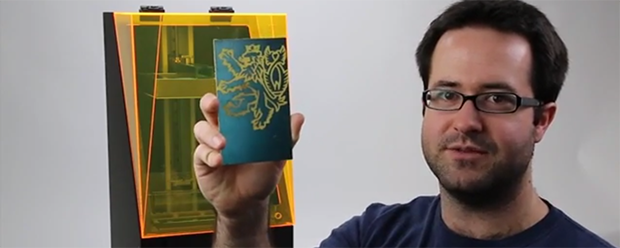
The folks over at Full Spectrum Laser are Kickstarting their own 3D printer – a stereolithography machine like the Form 1 and B9 Creator printers. During their testing, they discovered a new application for these SLA printers that should prove to be very useful for the makers and builders using machines – manufacturing PCBs with UV-sensitized copper clad boards.
Full Spectrum Laser’s printer – the Pegasus Touch – uses a near UV laser and a galvo system to build objects in UV-curing resin layer by layer. In retrospect it seems pretty obvious a UV laser would expose UV sensitive boards, but this discovery simply reeks of cleverness and is a nice ‘value added’ feature for the Pegasus printer.
The Pegasus printer has a laser spot size of 0.25mm, meaning the separation between traces on Pegasus-produced PCBs will be just under 10 mils. That’s a bit larger than the limits of laser printer-based PCB fabrication but far, far less complicated. Making a PCB on an SLA printer is as easy as removing the resin tank and putting a sensitized board on the build platform. Draw some traces with the printer, and in a few minutes you have an exposed board.
We’d really like to see if this technique can also be used with other SLA printers. if anyone out there would like to experiment, be sure to send the results into the tip line.
Video from Full Spectrum Laser below.


In theory, any UV laser 3d printer should be able to do this.
Now lets really use our noggin here….come up with a uv curable resist that can be removed by solvent and eliminate one step. This would allow you to create circuits on ANY copper coated surface…not just presensitized board….by not having to develop you reduce drastically the chances for bad results.
I like “POSITIV 20” resist for that job (can also be used to produce stencils) from CRC Industries:
http://www.crcind.com/wwwcrc/tds/TKC3%20POSITIV20.PDF
I like placing extra pieces of bare boards around my work piece before spraying. That way you get samples with a representative resist thickness. I expose these first to verify the exposure settings.
I’ve used positiv 20 in the past with excellent results. Is there a distributor in the USA for it? I can only seem to find dry film. thanks!
No, they banned some key ingredient in the US some years ago over some environmental blahbidyblah. A shame really.
Yeah! Profit before people! Wilful ignorance FTW!!11!1!
Love West Virginia
Is there really a need for a single sided PCB UV exposure unit anymore?
I can do this with a tanning bed.
“I can do this with a tanning bed and a laser printed transparency sheet of the traces.”
FTFY
This 3d printed isn’t being used as an exposure unit. It’s being used as a photoplotter. No mask necessary.
That said, I will _never_ buy from Full Spectrum.
Why not just use bare board coated with resin and create the resist layer directly? After etching and removing the resist you could coat and then create a solder mask as well. Hell’s Bells…then you could create a silkscreen layer on top of that… widen your field of focus a bit…
But that would lead to fuzzy prints… ;)
(Also, I hit report instead of reply, sorry. It’s been a very long day.)
Neat, but useful?
Currently I print my board on two transparencies, then aligning them on the UV-sensitized board, then placing whole thing under a UV light source. Two minutes of work followed by five minutes of wait?
This new method would have me remove the resin tank, align and mount the PCB to the build platform (double sided tape?), convert my gerbers to a jpg/bmp, then finally print to the 3D printer?
IF it’s saving time/money, it doesn’t appear that significant. Maybe if mounting and aligning the PCB was very quick and easy? Although I’m imagining a frustrating process involving double-side tape and wasted copper clad trying to correct the alignment.
Can the copper clad be the build platform for this resin? Does this resin dissolve with etchants?
In all likelihood, you would build a special jig that gets mounted inside the tank and allows you to set the PCB at the 0,0,0 point.
There would be no need for mounting tape as the no contact function of the laser and a level bed means that the PCB will stay right where you put it.
I agree with the people saying that this isn’t an improvement over existing UV processes. However it’s a kinda cool thing to do with your new 3D printer so fits perfectly as a hack.
However FS don’t exactly seem to have a great reputation when it comes to supplying their existing laser – which also started out on Kickstarter but is now a commercial product. That wouldn’t fill me with confidence about backing them on this.
From personal experience with the company I can say that their reputation is well-deserved. Avoid.
It’s to bad that the people who pledged to their current product do not have that same perspective. They have already raised 4 times their stated goal.
Why is KickStarter allowing them to run another project if they did not fulfill their previous one in a timely manner? That alone should cause a no go.
Why not simply put an UV laser diode in any of the plotter, router or engraver hacks?
I think it will allow better accuracy.
You could put a 405nm diode in a old pen for a HP plotter that has sheet feed capability or deliver it via fiber.
Inversely, I have though about using my UV YAG laser cutter to do stereolithography.
Lol, that lion is Czech national symbol, he literally took it from our national emblem :-D Just fun fact
how can we make our uv resin
I’m working on custom software for the pegasus touch. I think something like this would be easy to do. I have control of the hardware, just need to finish writing the software to do something useful with it and not just “laser” shows.