A lot of hackers take the “learn by doing” approach: take something apart, figure out how it works, and re-purpose all of the parts. [Henrik], however, has taken the opposite approach. After “some” RF design courses, he decided that he had learned enough to build his own frequency-modulated continuous wave radar system. From the level of detail on this project, we’d say that he’s learned an incredible amount.
[Henrik] was looking to keep costs down and chose to run his radar in the 6 GHz neighborhood. This puts it right in a frequency spectrum (at least in his area) where radar and WiFi overlap each other. This means cheap and readily available parts (antennas etc) and a legal spectrum in which to operate them. His design also includes frequency modulation, which means that it will be able to determine an object’s distance as well as its speed.
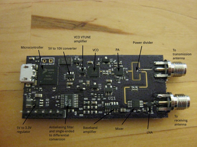
There are many other design considerations for a radar system that don’t enter into a normal project. For example, the PCB must have precisely controlled trace widths so that the impedance will exactly match the design. In a DC or low-frequency AC system this isn’t as important as it is in a high-frequency system like this. There is a fascinating amount of information about this impressive project on [Henrik]’s project page if you’re looking to learn a little more about radio or radar.
Too daunting for you? Check out this post on how to take on your first radar project.


Super sexy! Can’t get the project page to load though.
The link works for me, though his link to the MIT radar seems to be dead.
Truly excellent post by [Henrik], so elegant. (claps)
Awesome! Is there a BOM and aprox. cost for this project anywhere? I didn’t see one, maybe I didn’t look well enough.
I’m guessing about €50. The components are visible on the schematic.
Nice, thanks!
Quite interesting! I do find some of the design choices perplexing though. For example $60K software is used to design around an incorrect choice of connector which would cost very little to fix. With the PCB I would have made a separate PCB for the RF bits and the baseband/digital such that such thin traces didn’t have to be used and that it could be done on a two layer board, also at 6GHz traces should be silver plated for lowest loss. Improved S11 in his antenna could be increased losses with respect to simulation, tin does not sound like a good conductor? and PEC is used in simulation. I think you can build horn antennas by soldering sheet copper together if you are looking for a cheap way to make them?
In a 4-layer board, you do have the freedom to use all 4 layers or skip some… Simply leave the mid layers blank and a section of the board would be like a 0.062″ 2-layers. The problem with 0.062″ is that a 50 ohms trace may be a bit too thick to be practical. So may be that has to be a thinner 2 layers one.
And don’t forget, this is his first serious RF PCB design.
Wrong connector? Please elaborate on why you don’t like SMA’s.
This is a very sexy design. You can, however, improve the design by using quarter-wavelength stubs https://en.wikipedia.org/wiki/Stub_(electronics) on the power run to the amplifier (and to a lesser degree, the LNA) to prevent RF feeding back into the circuit. Note the amplifier bypass capacitors; you have to be careful with them, capacitors have inductance too! You don’t want your bypass capacitors to resonate about the frequency (or any nearby harmonic!) of the transmitter frequency. One way to deal with this is by using a quarter wave stub in a 90 degree trace-turn prior to bypassing high-powered RF components.
I don’t see the problem with SMA connectors on this, since SMAs are rated for at least DC – 18GHz. I personally would emit (and receive) using stubs on the board, and then mount the board on the arm of a dish. My concern is hosing the impedance of the circuit with the way you connect to the SMA.
What gets me is that there’s got to be a better way to get the mixer signal off of the output without cutting the power in half. I’m thinking some sort of parasitic stub antenna sitting beside the PA_RFOUT trace, which could then go straight to the SMA/antenna…
Oh yeah, the HMC219AMS8 is obsolete, use HMC218BMS8GE instead. The SST11LP12 is NRND, and they do not give an alternative, and what’s even more infuriating is that their “similar devices” list is populated with NRND devices as well, with the only exception being a 2.4 GHz amplifier. Skyworks seems to have some workable solutions, from a glance the SE5005L seems quite promising, as it also integrates the PA_EN circuitry, allowing you to get rid of the Q1 fet. Its input power is a whopping 12 dBm which means you can lose the attenuator U5, however the rated frequency range extends only to 5.75 GHz, but I’d be willing to try it up to 6. Furthermore, the DAC output from the MCU is likely to be noisy, and why waste the clocks pumping a DAC? Yes, I suppose you could DMA from a table of values, (if the MCU supports it) but… Why not simply offer a square wave from a GPIO and then integrate the output with something like what’s in this tutorial -> http://www.circuitstoday.com/triangular-wave-generator ?