A quick look at the pinouts of an Intel 8086 & 8088 processor reveals a 20 bit address bus. There was high demand for the ability to address 1 meg (2^20) of address space, and Intel delivered. However, a curious individual would wonder how they can achieve such a feat with only 16 bit registers. Intel solved this riddle by combining two registers so they could make it compatible with code written for the 8008, 8080 & 8085. The process they use can be a bit confusing when trying to figure out where to locate your code in the ROM. In this article, we are going to go over the basics of how the Physical Address is calculated and how to locate your code correctly in ROM.
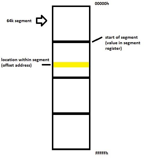
In a monumental effort to confuse young budding computer scientists in the late 70’s, Intel broke its 1 meg of address space into four 64k chunks, with each chunk represented by a 16 bit Segment Register. The value in a Segment Register, called the Segment Address can be thought of as the base address (0000h) of one of the 64k chunks. The address within the 64k chunk is found by an Offset Address. The combination of the Segment Address with the Offset Address is called the Logical Address, and can be transformed to form the elusive Physical Address. In a normal instruction fetch, the Segment Address is stored in the Code Segment (CS) register and the Offset Address is taken from the Instruction Pointer. So the Logical Address will be CS:IP or for example FFF0h:C000h.
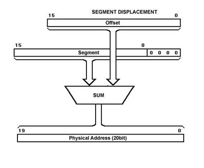
The formation of the Physical Address is done by multiplying the Segment Address by 16, and then adding it to the Offset Address. By multiplying the Segment Address by 16, you turn it into a 20 bit value by appending four zero’s to the right side. This calculation is done by a dedicated adder within the processor. But you need to know how the addresses in your program are turned into a Physical Address if you want to know where to locate the code in ROM. This will become more clear below.
The Reset Vector
Now that we are thoroughly confused about the extremely logical and straight-forward internal workings of the x86 address calculations, we can move on to why this information is useful. When the 8086 processor recovers from a hardware reset, the very first address it puts out is FFFF0. This means PINS A0 – A3 are LOW, and A4 – A19 are HIGH.
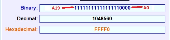
FFFF0 is the Physical Address. So the Logical Address would be FFFF:0000. With FFFF coming from the Code Segment (CS) Register and 0000 coming from the Instruction Pointer (IP) Register. These are the states of the registers upon reset.
Now, you might have noticed that FFFF0 is really really really really close to the bottom of our memory map. Indeed, it is only 16 bytes away. So the first instruction has to be a far jump to somewhere higher up in memory, and load the Code Segment and Instruction Pointer to the place where your program actually starts. What a brilliant design!
Why Knowing This is Important
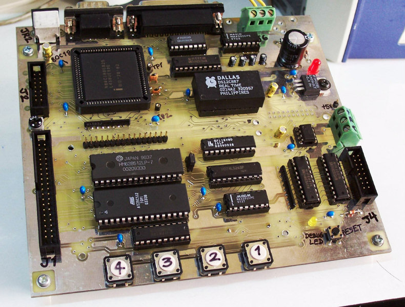
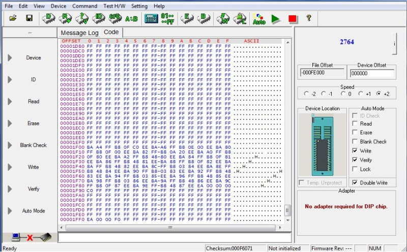
Want to roll your own x86 computer from scratch? Consider this schematic (pdf warning) from [Scott’s] 8088 SCB project. Take a look at the processor – he’s only using 16 of the address lines. For the ROM, he’s using a 2764 8k x 8 EPROM, which has 13 address pins. So the question is: where in the ^*#$ do you locate the code in the ROM??? Wait…is it…0000h? Ohhh no, that would be WAY to easy.
First, we have to figure out the reset vector address that will be placed on the EPROM’s address pins. The 8088 will put FFFF0 on its address bus. But from the hardware’s perspective, this address is actually 7FF0.
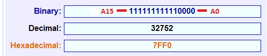
But wait, there’s more! The 2764 EPROM only has 13 address pins, A0 – A12. This means that when the processor puts FFFF0 onto the address bus, the address seen by the EPROM will actually be 1FF0.

If you still haven’t had enough, now is where you figure out how to get your code (with the reset instruction) into the correct place on the ROM. In this case, the FAR jmp must be located at 1FF0. This is generally done with what is known as a Locator – a program the strips the .EXE generated from the linker into something that can be loaded into ROM. There are not many of these programs around, and if you’re lucky enough to get your hands on one, please let us know in the comments. I have yet to locate Intel’s TLOC.exe, and Paradigm has ignored my requests for theirs.
Below is a hex dump showing the correct placement of the reset vector for [Scott’s] 8088 SBC. The EA hex instruction is a far jump. Far means outside of the 64k segment.
Anyone motivated to make their own x86 SBC now? [Wichit] made this 80C188 SBC, and provides a good starting point. I’ll stick with Arduino.
Note: The screenshots for the binary/hex converter came from here.


Frickin segmented memory. Ok now this brings me back.
Debug
A 100
*yikes*
back? this retro shit happens every time you boot your computer
even the latest 12 core 64bit 14nm monsters boot in this obsolete piece of crap mode, yay for intel backward compatibility …. :/
Right now I’m digging throught this freakin’ segment shit as I want to use one of my older PC’s for a hardware project. Just debugging a switch to protected mode to be able to use VESA linear buffer instead of the A0000 video buffer windows was a two week nightmare. I used to program 68000 in assembly and I expected the x86 to be tough but honestly I didn’t expect it to be this bad.
Save yourself the headaches and just use an ARM board.
The cost of the ARM board will easily be repaid in terms of reduced power consumption.
This, this and a million times this. It is the reason I despise x86 so much. Good to know that I don’t seem to be alone in this camp.
WTF? The backwards compatibility is one of the biggest strengths of x86.
If you really hate something for a few instructions executed before switching to 64 bit mode you should perhaps get some help…
The problem is that you can’t just have “a few instructions executed before switching to 64 bit mode”.
http://wiki.osdev.org/Rolling_Your_Own_Bootloader
I’d say that if you haven’t run away screaming in panic after reading that page and related articles, “you should perhaps get some help…”
According to that page, it’s just a handful of instructions, so what’s the problem exactly ? Of course, you also need to set up IDT and GDT, but you’d have to do similar things on other CPUs as well.
Anyone who thinks 1) bending over backwards so the streams don’t cross is just a few instructions and 2) other CPUs do it so it’s just dandy is brain damaged.
1) It’s a small price for compatibility. It only hurts 100 people in the world who write their own bootloaders, and 90 of them enjoy this kind of stuff anyway. 2) setting up page tables and other environment is not brain damaged. The settings depend on memory configuration that the CPU doesn’t know about. Requiring the programmer to set it up at the start of execution is simply the most sane thing to do. And again, it’s something that 99.9999% of the people never have to deal with.
That is why they are still around, when some better designs have never gained traction. Backwards compatibility is a bigger deal to the companies buying hardware and paying for software, historically FAR more important to them than the lower level complexity. What company would want to chuck all of their computer hardware and buy all new software, just to get some new feature in a completely different architecture? The million dollar question is when to drop something, and how far back to keep it compatible.
Most of the “better” designs weren’t actually better in the places where it mattered. For instance, the complex x86 instruction encoding is a good thing, since it offers better code density than RISC. And good code density allows better use of i-cache, which increases performance.
Wow, weird to think this is almost retro now. Nice article. One possible mistake:
“Intel broke its 1 meg of address space into four 64k chunks”
Should be sixteen chunks, yes? (Four would correct for the number of bits used in SR.)
(edit: would BE correct)
More accurately: they broke the address space up into 4096 chunks of 64K, overlapping by 16 bytes each :-)
1000h:0000h is the same as
0FFFh:00010h is the same as
0FFEh:00020h is the same as
…
0003h:0FFD0h is the same as
0002h:0FFE0h is the same as
0001h:0FFF0h
Yes, “4” is definitely wrong. :-)
That doesn’t seem right either. 4,096*64K=256MB! Are you thinking of an x86 processor newer than the 8086?
Jac’s right, and if you careful read what he’s saying you’ll realise he is illustrating the point that the segment base address and the index overlap each other by 12 bits. The upper 4 bits of the segment base address, plus 12 shared bits in the middle, plus 4 bits at the lower end of the index register = 20 bits in total (plus nearly one extra bit because of arithmetic carry).
Ok, now I see what y’all did there. Thanks!
He’s not quite right. It’s not that they overlap by 16 bytes. They begin 16-bytes apart. They overlap by 64k-16 bytes. Thus 0000:0010 is an alias for 0001:0000. There are 64k segments, each beginning 16 bytes apart.
No, the segment and index addresses overlap each other by 12 bits. I didn’t say the segment addresses overlap each other by 16 bytes. 64k – 16 bytes is another way of saying 12 bits of address.
Mostly I was responding to “Jac’s right”, and then going back to Jac’s comment about them overlapping by 16 bytes. I also probably wouldn’t say that they overlap by 12 bits, because they are additive and can impact more than the twelve bits, which makes the bitwise relationship of the bits in the middle a little less clear, but I take your meaning.
I think he’s talking about CS, DS, ES and SS, the four segment registers available on the 8086.
One of the things I hated about this scheme was that different segment:offset pairs could refer to the same memory location. What a mess!
Intel’s 8086 manual touted segmented memory as a good thing: you could modularize your code and data by putting it in separate segments.
Yah. I went with the 68000 microprocessor instead.
Yep, I was aghast when I found out how Intel did it. Getting 32-bits worth of registers to address just 1Mb in such a seemingly clumsy way, seemed crazy! The 68000 was a programmer’s dream come true :-)
On the other hand, intel’s method provided a nice upgrade path to the 386. With registers extended to 32 bits, this design works very well. Looking back, it’s actually quite amazing how intel managed to keep incrementally improving their design over several decades in rather smooth fashion.
I don’t see how this is a “nice upgrade path” compared to a flat address space. In fact, the 80286’s protected mode, where the segment register was shifted 16 bits instead of 4, broke some old code.
The 80386 supports a flat address space so why are you complaining?
Personally I was sad when AMD decided to remove segmentation in 64 bit mode – it made some kinds of microkernels much less efficient. And what did we gain?
. performance? Nope – x86 processors still need to support segmentation even under 64 bit mode (when running 32 bit programs) and actually using segments already was penalized compared to flat addressing.
. more efficient hardware? Nope. See above.
. extra opcode space by reusing segment prefixes (bytes that changes instruction interpretation located before the instruction proper)? No. AMD defined segment prefixes to be NOPs.
To add insult to injury AMD later included some simplified segmentation also in 64 bit mode. Intel doesn’t support it and the simplifications made it unusable except for the intended use: supporting virtualization. It still needs most of the complications of real segmentation.
So why would I like segmentation? It provides security with a byte granularity compared to paging (4kiB granularity), it supports doing fine grain security with some software support which means failures can be contained better.
The ‘386 has a flat address space + segments. That’s better than just a flat address space.
Intel’s upgrade path wasn’t upward compatible for either the ‘286 or ‘386 generation.
The ‘286’s memory model broke pretty much every practical 8086 program by replacing its predecessor’s address calculation of: Segment*16+Offset with LocalDescriptorTable[Segment].BaseAddress+Offset. This means that there’s no longer any relationship between an address such as: 0x1234:0x5678 and 0x1235:0x5668. The only programs that will therefore work are small model programs that didn’t use descriptors at all. Which is to say – it’s not upward compatible – a 286 operating system must map linear virtual-mode addresses to linear physical addresses to maintain 8086 compatibility.
The ‘386 essentially layers a proper paged virtual memory model on top of the broken ‘286 memory model. However, again, 8086 programs can’t simply be run in 32-bit mode because (a) The segment registers still map to descriptor tables (b) Segment registers are 32-bits and (c) The switch to 32-bit mode changes the interpretation of all the instructions that operate on 16-bit data to operate on 32-bit data. Intel ‘fixed’ this by creating a virtual 8086 mode for the processor, a hardware emulator for 8086 real-mode software. Which is to say, it’s not upward compatible.
The really disappointing thing is that it’s not hard to imagine how they could have made the 286 genuinely compatible by layering a paged memory model on top of 8086 segments. For example, addresses could then have been calculated as:
VirtualAddress=Segment*16+Offset, then
PhysicalAddress=PageTable[VirtualAddress>>12].Translation*4096+(VirtualAddress&0xfff).
That way, the segment/offset relationship is preserved as is the 286 physical address space. 286-specific programs could then be defined as Segment*256+Offset, which would give a 16Mb virtual address space, plenty of space until the arrival of the ‘386 and even up to the mid-1990s.
A page-table scheme such as the one above, would have executed protected 8086 and 286 code faster than descriptor-based virtual memory, even if this 286 only cached a single page table entry per segment (the real 286 cached a descriptor per segment). That’s because (a) >64K programs must often reload or modify segments, but a page table implementation would have resulted in fewer page faults and (b) ‘286 page table entries could have fitted into 32-bits [12-bit translation+12-bit Length+8-bits for attributes], so page faults would have been quicker.
Depends what you were trying to do, if you were a low-level assembly coder then segmented memory was brilliant. Different segment:offset pairs referring to the same memory location allowed for some highly-optimized code involving overlapping segment pages. And splitting the addressing across two registers allowed for some extremely fast texture mapping code where you’d use a segment register (e.g. ES) to reference the texture page while the offset BX (split further into BH:BL) referenced U and V. There were lots of other bit fiddling tricks you could use it for as well.
“Different segment:offset pairs referring to the same memory location allowed for some highly-optimized code”: I suspect that was more a happy accident than anything intentional on Intel’s part.
No, that was very much by design. And intuitively you would expect there to be a good reason, given that calculating a physical address with a 4-bit shift and a 12-bit add take more silicon and code than a single 16-bit shift. The purpose was to future-proof 16-bit applications and provide a simple way of mapping virtual memory to physical memory (with 16-byte granularity) in preparation for the switch to protected 32-bit architectures and proper page mapping. By allowing the segments to overlap you could pack all of a program segments into a single block thus greatly reducing memory fragmentation and the chance of apps trashing each other’s memory space. The optimizations I mention were hacks that game developers like myself used at the time and they broke the minute you tried running your code in an extender. We weren’t really supposed to use them, but everyone did anyway. :)
Sorry Bob, I misread. I thought you were talking about segmented memory itself. Yeah, I suspect the bit hacks weren’t part of the original plan myself :)
The image at the beginning of the article shows he’s using an Atmel AT29C512, which is a 64KBytes flash chip. It also appears that he’s using an Hitachi HM628512 SRAM chip, which has 512KBytes.
The article seems somewhat confusing. Firstly, the conventional way to decode memory is to allow memory to be mirrored at multiple addresses. So, if you have a ROM on an 8086, it must be possible to decode it at $FFFF:0000 (physical $FFFF0), because otherwise the processor won’t see the ROM when it resets. Therefore, it must be valid to address the ROM at $F0000 (if 64Kb is really decoded), or $FE000 (if 8Kb is really being decoded). And that means that a far address of $FFFF:0000 is just as good.
Decoding just 13 bits from 20 bits just means that the top 7 bits are masked out and the ROM will be decoded at every 8Kb region. There’s nothing odd about that.
Secondly, the article’s description of 8086 addressing is a bit confusing, because it says that the 1Mb address space is divided into 4x 64Kb segments. And that can’t be true, since 4x64Kb = 256Kb, not 1Mb. So, here’s a correct, and easier description:
*****************************
The 8086 has a 1Mb physical address space: $00000 to $FFFFF . However, all the main address registers: IP (the instruction pointer, PC on other processors); BP, BX, DI, SI and SP are all 16-bits, which only allows 64Kb to be easily addressed.
So, what Intel did was to create 4 extra 16-bit ‘segment’ registers: CS, DS, ES and SS. Then whenever the processor needs to address memory, it picks a segment register (e.g. DS) and an offset (e.g. BX) and then calculates the address as:
Segment_Register*16+Offset. In this case it’d be: DS*16+BX. This gives an addressing range up to $FFFF*16+$FFFF=1Mb+64Kb (the top 64Kb just wraps around to the bottom of memory on an 8086). Because some of the address bits overlap in the calculation, it means that multiple segment:offset values also map to the same address. For example: $0010:1234 maps to the same address as $0011:$1224, because $10*16+$1234 = $11*16+$1224.
The 8086 and 8088 pairs each address register with a default segment register. IP is paired with CS by default, BX and SI are paired with DS by default, DI is paired with ES by default, BP and SP are paired with SS by default. However, by using ‘segment prefix’ instructions just before a memory accessing instruction, you can override the default. For example, SEG CS:MOV AX,[BX] would copy the 16-bit value at CS:BX to AX instead of using the location DS:BX. In any case, the four segment registers mean that the 8086 has easy access to 4*64Kb = 256Kb.
To gain access to the whole 1Mb you need to muck about with the segment registers’ contents. For example, MOV DS,1000 would now mean that the data segment would reside at segment 1000. That’s clumsy, but the 8086 also has some specialised jump far and call far instructions that load a new CS and jump offset in one go.
*****************************
Correction: MOV DS,1000 isn’t strictly possible. You can do MOV DS,byte ptr[1000] to load DS from a memory location. Or you can do e.g. MOV AX,1000 then MOV DS,AX or do POP DS to pop a 16-bit value into DS. However, loading DS with a constant isn’t in the instruction set.
+1 interwebs for this guy, for a MUCH better explanation.
Thanks- The original article needed some clarification. Right off the bat: ANY time you are talking about “Meg” and “K” or any amount of memory whatsoever, and are not specific about Bytes “B” versus bits “b” you are already causing trouble!
Hello world in DEBUG:
DEBUG
A
MOV AH,9
MOV DX,108
INT 21
RET
DB ‘HELLO WORLD$’
R CX
14
N MYHELLO.COM
W
Q
Nice. I was sad when they took Debug out of Windows. I think they took it out in 7, but maybe it was Vista.
It’s look like a locator is available from here http://geezer.osdevbrasil.net/johnfine/
680×0 fanbois: “Why would you EVER want a processor that can only address 64K at a time???”
808x fanbois: “Why would you EVER want a processor that throws a fit if a word is not stored at an even address???”
Yeah, this sure brings back memories of the 1980s…
“808x fanbois: “Why would you EVER want a processor that throws a fit if a word is not stored at an even address???””
If memory serves, just putting a CNOP 0,2 instruction before any data chunk would align everything at an even address ensuring safety.
There are situations where you can’t align your data properly. For instance, a network packet with different fields on different alignments. In those cases it’s very useful if the hardware supports unaligned access, even at a performance penalty.
Hi,
for anyone who wants to dig into the old rusty x86 and isa architecture
There is a book by “Ed Nisley” called “The Embedded PCs ISA Bus” where he actually describes how to “µController” an 8088/8086 because these early CPUs are simply to hack because you just connect a bunch of TTL 74LSXYZ ICs to it and you have fun. Btw. the book ist LEGALLY free for download at his blog-site:
http://softsolder.com/2011/10/03/the-embedded-pcs-isa-bus-firmware-gadgets-and-practical-tricks-unleashed/
Then there is one from archive.org
https://archive.org/details/ISA_System_Architecture
What’s really cool is “ISA System architecture” by Tom Shanley/Don Anderson
because, the x86 memory adressing system plays on the ISA bus (8086 / 80186 / 80286)
The tragic flaw of the ISA bus is that the IOCHRY signal is active high
The ISA bus (or slight variations thereof) is still in widespread use in microcontrollers, typically for Ethernet and LCD interfaces. You can even program a FT2232H USB peripheral chip to talk to ISA bus peripherals.
The ISA bus also supported DMA which was almost never ever used except for an obscure command in Microsoft BASIC.
DMA was very much used for sample playback/recording on ISA soundcards… Even some joystick interfaces used DMA.
Also used on some of the old Ethernet card, Floppy drive controller card and some fancy Parallel port cards etc.
Thanks! I’m trying to build an ISA extension card as ISA seems to be fairly simple to interface. I enjoy playing with these old but simple technologies a lot and I’d like to re-use some of the old PCs for simple control/measurement. I can’t imagine myself building even a PCI card not to mention PCI-Express. The difference in the complexity seems to be enormous.
PCI is not too out of reach with the help of small CPLD. There are POST diagnostic cards from China that have only 3 GAL chips – 1 for the PCI and 2 for the 7 segment display decoder/driver.
See here for a PCI project with full write up using discrete parts: http://elm-chan.org/works/pci/report_e.html
The component count can be reduced by using a modern XC9500XL series CPLD.
PCIe on the other hand might get a bit more difficult as having to deal with high speed serial signals. I haven’t seen any FPGA/CPLD part that have SERDES without going to a BGA package.
BTW you can also hack a $5 PCI Ethernet card that has a 32-pin DIP socket for boot ROM (as long as it supports writing to FLASH chip). From there you have a large block of memory space with the usual address, data line and async control signals.
Hi,
here is another one, uses simple i/o
http://linuxgazette.net/124/dutta.html
74lsXXX logic? We used a GAL20v8 instead (basically a CPLD). It saved a ton of wiring and made modifying the system much faster/easier. Once I got a taste of using the CPLD, I never went back to using discreet logic.
probably the most annoying hack in PC history. for further information: http://en.wikipedia.org/wiki/A20_line
if you’re into that kind of stuff, have a look at the ” IBM PC/XT Technical Reference manual”.
Back in the day, stripping the exe header off to make .com files was done by using exe2bin. Looks like this still comes on modern day windows machines.
you may also want to get an old version on turbo/borland c from embarcadero (free on their site somewhere…) and use tlink to link into a .com file.
UGH! That RTC, the DS12C877, what a hog that guy is. I still have to deal with some equipment that has a similar chip from ST in it, but it’s static ram along with a built in RTC. The reason it’s so fat is that the hump contains the crystal for the clock and a backup battery for retaining memory and the time when the power fails. High failure part and will soon go the way of the dinosaur, which presents a whole new challenge… There was some old gaming console around that had the same chip and some guy figured out that you can dig into the package and find the battery terminals and hack in a new replaceable coin cell, but it’s not really worth it.
Backward compatibility rocks!
I just finished a small arcade game project using a “junk” 2007 dual core Dell AMD motherboard with 1GB ram to fit into an arcade case, The hardware is incredibly overkill just for a 1983 DOS game but old PC’s are effectively landfill, total cost was just my time and a crap load of messing about to get it all to fit in the cabinet and pulling the keyboard apart to fit to the arcade buttons.
Check list,
Hardware: Free
Operating System: FreeDOS: Free
game with source code modified slightly for arcade use: Free (digger.org)
Even if you could get a 8086 that is hobbiest friendly or squeeze it onto an arduino board why would you even bother?
I remember reading about this in BYTE when the 8088 first came out. I immediately realized that Intel was doomed, the 68k would take over the world, so I would never have to worry about this abomination.
Yes I’m old, but at least I’m not foresighted.
I did a lot of this for a class in college. I may even have the compile tools stored somewhere as I spent many 2am nights coding for my class. I’ll have to take a look this weekend.
Why didn’t intel just make a 32 bit address?
It could even use less transistors considering the lack of adders and stuff, as it would almost only be two registers.
Tho it might be because of wire-bonding and other off chip stuff.
Hm, because this would likely break compatibility with older x86 CPUs?
I think the problem was the number of pins on the package. The 8088 I was using already had 40 pins in a through-hole DIP package. Back then, you didn’t find more than 40 pins on an IC, generally speaking, and surface mount technology wasn’t so common. Adding another 12 pins would have been very difficult.
microchip PIC?
time to break out the pink shirt book then is it ?