You don’t need to look very hard to find Nordic’s nRF51 wireless module; it’s found in hundreds of products and dozens of projects over on hackaday.io. The nRF51 is a SoC that includes an ARM Cortex M0 processor and a variety of radios for Bluetooth and other protocols. Useful, if a bit limited in processing power.
Now, Nordic has a new SoC. It’s the nRF52, a Cortex M4F processor, a Bluetooth radio, NFC, and a bunch of Flash and RAM to make just about anything you can think of possible. Yes, it’s an upgrade to the nRF51 – a better processor and NFC, and all the possibilities that come with that. Currently there’s only one part and two package options: a 6x6mm QFN48, or a wafer chip that will be covered with impregnable goo.
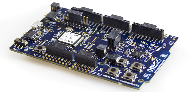
Already there are SDKs for IAR Workbench, Keil4 and 5, and gcc. The SDKs won’t help you quite yet; it’s not available through the usual distributors yet, but the nRF52 Preview develoment kit is. That’s a single board development kit for the nRF52, with Arduino pinouts and Mbed support.
Thanks [Alvin] for sending this in from Trondheim.


Too bad it costs 76 dollars. http://www.digikey.com/product-search/en?x=0&y=0&lang=en&site=us&keywords=nRF52
That’s $76 for the whole dev kit. Not just the chip.
Sounds good at first glance, but running a pure software bluetooth stack (extremely hard realtime) on the same processor as the app? No thanks…
The most common applications for BLE can deal with periodic interruption to handle the radio, and even then the radio on these things does most of the time critical stuff for you. The radio handling task doesn’t need to be high priority.
If your application can’t handle that, add a second micro to this or use a fixed-function Bluetooth radio.
The radio on this doesn’t do much for you at all, timing-wise. Once you have multiple links, the software will be doing quite a lot…
I’ve worked with the predecessor to this chipset, nRF51, which has a similar architecture. They have exceptionally well written, mature (the base stack is at version 8, is several years old, and is continually being improved). It is entirely interrupt driven (when the stack is enabled, all stack radio and timing interrupts are higher priority), well documented in terms of timing of those interrupts, and has protection between the stack code / resources / peripherals and application code / resources / peripherals. It sounds like it might be difficult to manage on the same chip, but in practice it’s really not that bad, and they have very extensive documentation. The single processor solution likely reduces power consumption noticeably as well (if you’re doing BLE for a reason, it’s probably going to be for power savings). If you want a hobby “Bluetooth” application that’s easy to hook up, buy a Bluetooth-to-serial module (or BLE-to-proprietary serial) with a coprocessor and be happy with that… You can always set up the nRF5x chipset to be an SPI slave (there’s demo code for that) to a coprocessor, as well.
If you need very good realtime control, things get more difficult, however. The new M4F processor is much faster than the M0 in the nRF51 series and has faster interrupt performance, so this is less likely to be an issue. I had an application where I needed fully non-interrupted execution for a block of time to bit bang a pretty non-standard requirement, and there are even APIs for requesting a guaranteed, non-interruptible timeslot (for say, the 10ms you need to be uninterrupted) from the stack. This slot is timed to guarantee that you do not cause the stack to lose a BLE connection. The stack is of course Bluetooth compliant and approved, so it does in fact work…
To give you a better idea of how capable this stack is of realtime operation, that timeslot API is designed for applications that need to use the 2.4GHz radio for a proprietary protocol AND standards-compliant BLE in the same application. And yes, they have sample code of this working.
Not a Nordic employee, btw. After a lot of shopping around for MCU+BLE single chip solutions I settled with the nRF51 and I was quite happy (Other than TI I think only Dialog and CSR might be worth mentioning). The CC254x is a disaster in terms having your application and BLE on the same chip; you basically need to buy IAR, as there are no open-source compilers that support the architecture without a lot of work that no one’s bothered to publish (an 8051 + SDCC guru might be able to figure it out). TI has a new pretty ridiculous chipset that has three (M3, M0, and a proprietary low complexity, low power processor) on the same chip, but I haven’t tried it yet. Power specs are not as good as the nRF52, unsurprisingly, given how much stuff is just on that chip. I will say the peripherals are much nicer on the new TI part, but I’m not all that confident in their stack quality from the comments I’ve seen online about their previous generation part…
NXP is also likely coming out with a few new decent parts, having bought out another BLE company…
thirtyone wrote:
>TI has a new pretty ridiculous chipset that has three (M3, M0, and a proprietary low complexity, low power processor) on the same chip, but I haven’t tried it yet. Power specs are not as good as the nRF52, unsurprisingly, given how much stuff is just on that chip.
At first I thought so too. But then I started digging into the datasheets and try to compare apples vs apples, and things might not be that simple:
– E.g. the sleep current consumption of both chips (i.e. everything off except an 32kHz RTC timer and RAM retention), you will see that TI’s CC2640 has lower current consumption than the NRF52. This parameter is important in many applications where the CPU is inactive for longer periods, as will help you get a lower average power consumption.
– E.g. the RX current consumption for demodulating 1 Mbps Bluetooth Low Energy (Bluetooth Smart) with NRF52 is higher than with CC2640, and the NRF52 RX sensitivity performance is not as good as the TI radio chip.
– But in TX, the NRF52 seems to use less power than the CC2640, measured with same TX output power.
Alright, so the NRF52 is not a real product yet, but just a “preview SoC”. When it is out for real (perhaps summer 2016?), they might improve some of its specs?
PS: Why haven’t Nordic Semi announced any ULPbench [1] score yet to highlight how low power their new 55 nm NRF55 chip is? They announced all the CoreMark score, which measures CPU performance, and those scores are of course really high, knocking the competition out of their socks. But we don’t only need the chip to have CPU muscles — it needs to be low power too. Do you know if anyone with a dev kit has tried to measure it?
[1] An MCU power consumption benchmark test — https://www.eembc.org/ulpbench/
Why cant they release these things as a software switchable source/sink? Instead we get 95% of them as sinks and it’s pulling teeth to find any that have the Source firmware loaded.
Hi Tim,
I’m new to this so what do you mean a sink in terms of a soc?
Source/sink are Bluetooth-specific terms. A source transmits audio/video, a sink receives it. Bluetooth headphones are an example of a sink.
Source/sink are general streaming terms. This is BLE, so where BR/EDR would be master/slave, the terms are central/peripheral.
They have it already (for the nRF51, anyway):
https://developer.nordicsemi.com/nRF51_SDK/nRF51_SDK_v8.x.x/doc/8.1.0/index.html
The S130 SoftDevice supports both central and peripheral… I do hear it’s buggier than the Peripheral version, which as you say 95% of people use and is probably best supported.
IIRC those softdevices are behind a login/serial-number-wall; you might need to buy a dev kit first to get access to it (that $80 kit comes with a debugger onboard as well, so I’d say it’s worth it?)
My guess for why it’s so much more expensive than most of your high demand mass market dev kits these days is because they didn’t have the development time to design their own debugger, like TI and STMicro. It’s an integrated ST-Link debugger on-board, which only works on Nordic parts, but can do full speed debug and programming of external Nordic boards.
The initial softdevice is S132 and is included in the initial SDK. You can find it here: https://developer.nordicsemi.com/nRF52_SDK/nRF52_SDK_v0.x.x/
Nordic changed their policy on access to technical info about 6 months ago, and got rid of all the login/serial number requirements.
To me, there are a lot of esoteric looking parts in the photo of a board, in the means of the pin headers and connectors. What is going on here?
Those pinheaders still have their pick-and-place caps on them. Otherwise the pick-and-place machine cannot pick them up.
76 bucks for a dev kit is a lot, I’d be interested in spinning a cheaper board and pooling in with fellow hackers to get it cheap.
Nordic kits tend to be pricey, though the equivalent for the nRF51 was $100 when it came out so I guess this is progress. There are a number of mbed supported full devkits for the nRF51 that are under $30, and if you’ve got an SWD debugger you can get breakout boards from China for $6.
I suspect we’ll see the same happen for this new part.
On the other hand, $76 is a drop in the bucket compared to what the Bluetooth SIG charges for licensing to sell anything (including unfinished devkits!) with Bluetooth.
sounds like a good project idea to me…. if only I had the time
Most of that $76 is the integrated SWD debugger (by Segger). I’d love to see this happen, but either you’re going to end up doing a programming-only board (parallel or whatever), which you can already buy from China for nothing (for the nRF51 series right now, anyway) or an SWD ARM debugger with software to bridge to GDB, which I have yet to see a hobbyist group have the experience/time to design correctly. Half the documentation is behind Nordic’s registration wall anyway, which has required a valid debugger serial number.
This board also doubles as a “j-link” programmer / debugger for use on your external target board. This is accomplished by attaching the target board to the connector located at P19. This is a 10 pin Cortex m series connector 0.05. (Upper left in the picture on top of this page. Programming may also be achieved by connecting to P20. The board also comes up as a “flash drive” where you can drag and drop a compiled hex file and it will program the part for you without the need for any other programming utility.
One other thing that has not been mentioned is that this device not only runs a fully qualified BlueTooth Low Energy Stack, but can also run the ANT stack and a propriety stack of your own design. As the stack is located in flash it can be updated (as well as the application) by OTA or via the UART interface.
embedded flash in the SoC vs SoC with external spi flash ..
which is better??
Generally speaking, embedded will be at least as good as external SPI. In the ‘worst’ case, the embedded _is_ SPI flash, just on-die (or in-package in the case of stacked flash). In the best case, it’s QSPI or even fully parallel.
To save someone the effort of finding out some basic specs on what “a bunch of Flash and RAM” means:
512 KB flash
64 KB RAM
64 MHz clock
DigiKey sell this for 32$. Donno, where you’ve seen 76
http://www.digikey.com/product-search/en?KeyWords=NRF52-PREVIEW-DK&WT.z_header=search_go
I followed that link and the price is $76. Dunno where you’ve seen $32.
Wow, a chip company is actually making a part to serve the market in a timely fashion! That’s totally wacky.
I mean, TI *owned* the 802.15.4 radio market for a while, and the MSP430 was a great alternative to the PIC/AVR wars, and was excellent at low power and small footprint …. and, yet, they never combined a ChipCon radio and an MSP430 into an SoC.
TI could have been 6 years ahead of the game on this IoT fad, back when it was called “Smart Dust”, but they just decided not to be. Amazing.
They did! the CC430 series (for ISM 900/2.4GHz) or the CC25xx for BLE!
IIRC the first release was a disaster (insane list of chip errata, pretty much half usable without a lot of workarounds). They used to have a really cheap watch dev kit with that SoC (EZ-430-CHRONOS). I think that was about 6 years back, and showed up on HaD a few times. Ended up designing in cheaper 2.4GHz modules and separate ICs.
I’m starting to work with the BL652 which is based on the nRF52 SOC. I’m bypassing the SmartBASIC offered by Laird Tech, and using the Nordic SDK, cmake, gcc ARM cross-compiler, etc. I’ll let you know how it goes!