CMOS imaging chips have been steadily improving, their cost and performance being driven by the highly competitive smartphone industry. As CMOS sensors get better and cheaper, they get more interesting for hacker lab projects. In this post I’m going to demonstrate a few applications of the high-resolution sensor that you’ve already got in your pocket — or wherever you store your cell phone.
CMOS vs CCD
First lets quickly review image sensors. You’ve probably head of CMOS and CCD sensors, but what’s the difference exactly?
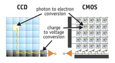
As the figure above shows, CCD and CMOS sensors are both basically photodiode arrays. Photons that hit regions on the chip are converted into a charge by a photodiode. The difference is in how this charge in shoved around. CCD sensors are analogue devices, the charge is shifted through the chip and out to a single amplifier. CMOS sensors have amplifiers embedded in each cell and also generally include on-chip analogue to digital conversion allowing complete “camera-on-a-chip” solutions.
Because CMOS sensors amplify and move the signal into the digital domain sooner, they can use cheaper manufacturing processes allowing lower-cost imaging chips to be developed. Traditionally they’ve also had a number of disadvantages however, because more circuitry is included in each cell, less space is left to collect light. And because multiple amplifiers are used, it’s harder to get consistent images due to slight fabrication differences between the amplifiers in each cell. Until recently CMOS sensors were considered a low-end option. While CCD sensors (and usually large cooled CCD sensors) are still often preferred for scientific applications with big budgets, CMOS sensors have now however gained in-roads in high performance DSLRs.
Imaging DNA
It’s always interesting to see how much can be done with CMOS sensors though. A recent article described the imaging of single molecules of DNA stretched on a surface using a mobile phone camera. These results are pretty impressive when you consider that each fragment is only 10 microns long (0.01mm). The researchers 3D printed an attachment for the phone which included a blue excitation laser. This laser was used to illuminate DNA which had been stretched out on a surface and stained with a fluorescent dye. When illuminated the dye lights up green and passes through a filter and magnifying lens where it is detected by the phones camera.
While this is one extreme, others have suggested using cheap mobile phone based microscopes for pathogen detection, and a cheap mobile phone based fluorescent microscope would make a neat hacker tool (I know a number of people are considering kickstarting just such a project, so if you’re interested leave a comment below!).
General-Purpose Microscopy
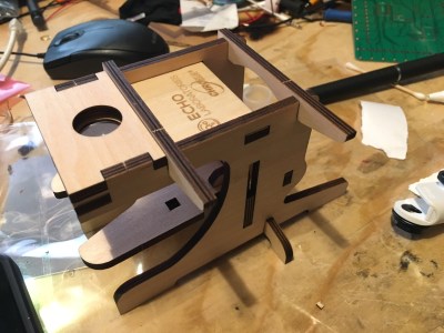
However, if you’re less interested in fluorescence and more interested in a general purpose cheap microscope, a number of other options are available. Inspired by Kurt’s post of his Echolabs phone microscope, I’ve been playing with his and other phone based microscopes.
I believe the Echolabs microscope was originally a freebie given away at tradeshows. However it’s now available from their site for $10. The microscope comes as a flat packed laser cut kit. While it can be a little fiddly to assemble there’s a great assembly video available and it shouldn’t take more than 15 minutes or so.
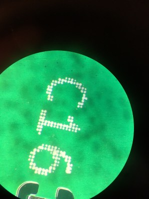
The project is great fun, and definitely and interesting project, but how good is its performance as a microscope. In order to investigate this, Kurt introduces the USAF1951 resolution target. The USAF1951 target is a slide on which is marked with features of ever decreasing size. I got mine from Thorlabs.
This target allows you to determine the smallest feature that you can resolve with your microscope. Somewhat ironically the target will cost you many times more than the Echolabs microscope, but if your interested in these things it’s a useful calibration standard to have around.
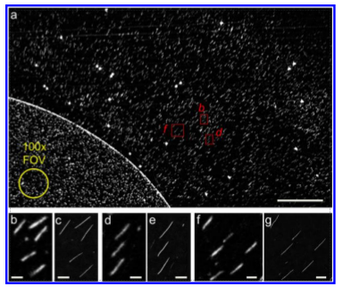
The image I acquired using the wooden microscope is shown below on the left. This is the inner set of targets from the USAF1951, the first level down. Like Kurt I was able to just about resolve group 5 element 2. Each line here is 36 microns thick (0.036mm). That’s not bad for $10!


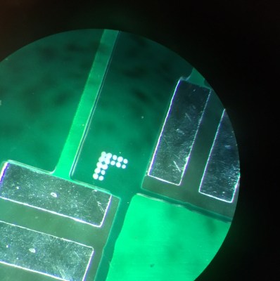
On a whim, and hoping to have a small inspection loupe which I could carry around, I also picked up an Olloclip macro pro lens. While I can faintly hear muffled cries of “that’s not a hack”, a good inspection loupe is an invaluable hacker tool. I also thought it would be interested to see how it performed with the USAF1951.
The image above right shows the USAF1951 target captured with this lens on the iPhone 6S. While significantly more expensive than the Echolabs microscope, the Olloclip shows that the iPhone optics can be pushed a bit further. All of group 5 is clearly visible and if you zoom in, group 6 element 2 can clearly be discerned. This is a linewidth of about 7 microns (0.007mm). Both the better illumination possible with the Olloclip, and the improved optics probably help.
Capturing Images from Your Traditional Microscope
While imaging micron-scale features is great fun, the microscope I use most often is a general purpose inspection microscope for inspecting components and SMD rework. Often I want to take a quick snap of a piece of work too, either to document my progress or highlight a fault. In the past I’ve struggled to jam mobile phones against the eye piece lens in order to take a picture. Surprisingly this kind of works, but it’s a fiddly and awkward process.
While I’ve used eyepiece C-mount adapters and cheap CCD imagers from Shenzhen. The results were less than ideal, and I often just want to take a quick snap and upload it. Surprisingly there are clamps which make the jam phone against eye piece process a little more robust (though they are surprisingly expensive). There has to be a 3D-printed alternative for this one.
Still, after some fiddling the clamp can produce quite reasonable images. The picture below shows 0.8mm pitch pins on a TQFP IC.
Hopefully this short review of phone based microscopy has given you some inspiration. I’d love to hear about more optics based hacker projects. How have you put your old cell phone’s camera to use? If you know of any cool projects, or are planning one, please comment below!


We used the lens from a DVD player focusing stage, stuck onto an iPhone camera, as a crude field microscope. Zoomed in, we were able to distinguish between two species of pant by measuring the size and density of the stomata. In fact, the results were good enough for publication (although of course we confirmed with a traditional microscope later on). Back-lighting helped, as did digital zoom. Amazing that we have access to such powerful technology!
That’s cool as hell. You basically MacGyvered science.
I have a lens setup just like this.
I briefly worked as a QA technician at the Cypress CMOS image sensor division in Mechellen, Belgium.
A lot of the CMOS image sensors they designed were military-grade and space-grade, and quite a few of the sensors i optically inspected ended up in actual space.
The article says that for scientific applications CCD is preferred, but i was told the opposite.
On the first day i had to watch 2 DVD’s that explained the design choices and manufacturing process, they were very technical. I have seen them on youtube too, let me see if i can find them.
CCD are preferred for scientific application because they use electronic shutter ( no need for moving part which might induce vibration and therefore deteriorate the quality of the image also obviously no wear and tear) and because of their sensitivity. however a typical lab camera costs a bundle offers only a few Mpix and the vast majority are still B/W.color CCD only started to show up on the market like 2 years ago and best in market nowadays is around 10Mpix and will set you back about 10-15k with the (obviously) proprietary “control software”/drivers.so sad to see that a lot of scientist really are not that tech savvy. for our purposes we didn’t need the sensitivity and opted for a 800$ off the shelf 21Mpix canon DSLR instead of an 14k$ 3mpix CCD lab
camera. added bonus since the sensor on DSLR is bigger you get a bigger field of view in the pictures which reduced our workload a lot. 4 years of heavy use later the camera shows sign of wear and tear but at that price range we can afford to change the camera every few years and are still much better off then with the lab cam……
ccd started to show up on the market like 2 years ago? ccd are preferred because they use electronic shutter? pile up more BS please.
Im working in a scientific environment and was talking about CCD IN SCIENCE not in general and if you read correctly i said COLOR CCD cameras showed up very late on that particular market NOT CCD sensors in general. and if you learned to read correctly i said mostly because of electronic shutter and sensitivity ( to a lot of spectral frequencies) and yes electronic shutters are a thing google it. they are used when no vibration/moving part is a requirement and also to avoid the rolling shutter effect in high speed applications. and in future learn to read and if you know nothing about the topic at hand STFU.
Whats the matter Snow, cant take a Mocking Jay? :P
@foo i have no problem with criticism but i have a problem with idiotic trolls who cannot read…..
For low-light applications (astronomy, fluorescence microscopy), CCDs were traditionally the preferred technology. The quantum efficiency of CCDs available in camera units has been 90+% for over a decade now. In the past 5 years or so CMOS QEs have made it into the 70% range, with 80-90% QE cameras becoming available in the past 6 months. This timeline is pushed up a little for things like satellites where you’re dealing with the bare chip and building around that, not a camera unit with a lens on one end and a USB on the other, but the same idea holds.
As the article mentions, the noise profile of a CCD is preferred for quantitative imaging over a CMOS as well. CCDs are more even in terms of read efficiency and offset per pixel thanks to sharing some of the amplification circuitry across the entire FOV. On CMOS chips the read-out and amplification is per pixel, so each one behaves just a tiny bit differently. In applications where this matters you have to correct for the ‘fixed pattern noise’ inherent in the chip read-out.
Of course the shutter properties (rolling vs global) matter for some applications. Clever applications actually take advantage of the rolling shutter and sync to the illumination laser so you’re only exposing your fluorophores that line up with the active pixels. I’m usually working in a regime where the physical dimensions of the chips is less of a concern (both in number of pixels and the pixel pitch) but the extra size and small pixel pitch on a CMOS chip can be a big advantage. Scientific CMOS cameras are typically 4-5 MP @ 4.5 micron pitch, where the biggest EMCCD is a hair over 1 MP @ 13 micron pitch.
Big winner for CMOS cameras is read speed. 100 fps at 5 MP/frame is typical. Need a big-ass pipe to pull that data off the camera and these are sometimes deployed on instruments who take images at max rate for a week straight. Like, you can start with a fertilized fish egg and watch (in 3D!) every single cell division that happens until the fish is big enough to swim out of the sample chamber. And you’re acquiring data at 1 GB/sec the entire time. It’s fun to describe this to the Uni IT department and watch their eyes start to twitch.
Oh, and CMOS cameras are half the cost or less of an EMCCD for almost comparable performance in the end.
Source: I build microscopes and buy lots of cameras.
That’s a lot of data generation! :) A ~0.5 petabyte storage array for a single instrument would be fun! I assume that a lot of data reduction happens on instrument.
Thanks for your comment, you have a lot more practical experience building these rigs, were as I’ve mostly just looked at the data that pops out the other end. I recently had a poke around inside a Genome Analyzer 2 which uses a CoolSnap K4 (in turn based around a Kodax KAI-4020) in a TIRF microscope. That as peaked my interest,
I’d love to hear more about the practical aspects of your rigs.
How to deal with that much data is a huge issue in research at the moment. Funding agencies say you have to keep the raw data for X number of years and some of them say you have to make it available for outside researcher to use. When an entire PhD thesis was 5 GB this wasn’t a big deal, but now that one paper can be 2 PB of raw data, what are you supposed to do with that? And do you have to keep all of the data sets that didn’t work? That’s deleting data! And scientists don’t arbitrarily delete data! *cue academic pearl clutching*. At the moment it’s still an unsolved problem.
Gene sequencers are secret caches of surplus microscope equipment. Most are basically a microscope in a big pharma-colored box. We have a pair in my lab that got fished out of the dumpster and have already yielded some nice components.
Been toying with the idea of putting more about our instruments online. Not sure what the best means to do it would be, but considering the number of 3D printed parts, Arduinos, and 80/20 extrusion we use I think it would fit in here pretty well.
I definitely be interesting in talking to you more about this over email. I’ve also been talking to a company working with some super-resolution techniques and it could be interesting to chat about that too if you are amenable. My email is new at sgenomics dot org.
i can’t find the videos anymore sadly, they had a lot of great insights into all aspects of the sensors.
The time i worked there was over a decade ago meanwhile, and i can confirm that many of them had electronic shutters and proprietary interfaces.
I have a couple of “Ultra Small Pocket-sized Handheld LED 45X Microscopes” on eBay ($1.50 w/free shipping) and I swear by them. They’re clear, easy to use, and lit.
Nothing beats something that you can carry around in a pocket that you don’t care if it gets beat up or broken. Nothing beats having a light source to improve the view.
I find these invaluable for reading the numbers on tiny ICs, doing trace inspection, and a zillion other things. There’s one on my desk right now, one in the workshop, and one in my kit at the hackerspace.
Another useful tool is the “Pocket 500X 2MP 2.0M USB 8 LED Microscope Video Camera” ($11 w/free shipping). They do exactly what they claim, and are useful for long-term inspection and image recording.
I use these for recording trace widths and other experimental results.
(On mine, I peeled off the base sticker and put a magnetron magnet from an old microwave oven, then glued felt to the bottom. It now sticks to metal surfaces very well, such as the top of my bench supply, and the extra weight makes it easier to manipulate.)
Stay away from Jeweler’s loupes that are opaque and unlit ($1 on eBay) because the shroud will throw the part into darkness. I have one of these and it’s pretty-much unusable.
I also have a high-end loupe with a removable transparent graticle. The sides are clear, so it lets light in to illuminate the object.
The resolution target is fine for testing the resolving power of your system, but having a transparent graticle allows you to lay the graticle next to things and easily show how big features are.
Here’s an example I made up for our hackerspace. Using the graticle, I can conclude that the “kerf” on our laser is 0.02 inches, about 20 thou.
(I used to make software for laser printers.)
My img link didn’t work, here’s another go.
Transparent graticle showing the spot size on our laser:
https://cdn.hackaday.io/images/2063331460400772760.jpg
If that didn’t work, click the link on my name to see the image.
And regarding optical experiments, the HAD prize team at my space is developing an optics bench that can be cut out with a laser cutter, with a boatload of experiments and features.
(And a woefully sparse .io project page at the moment, because we just started last Thursday. First build log is coming real soon now!)
Check out “laser cut optics bench” on Hackaday.io, or click on the sig on this post.
https://hackaday.io/project/10707-lasercut-optics-bench
Yep those cheap loupes with the LED are great! And ditto the comments about the USB microscope, though I’ve found some are better than others.
My favourite though for detailed wider shots of a PCB is a second use for my mirrorless (Sony A5000) which cost me about £150, so cheap for a good camera but not good value just for this.
But put on some £10 macro rings with pogo plugs to pass though the electronic connection and add a battery powered LED ring light and you have a optical stabilised, auto focus, power zoom 20MP microscope for effectively £30 assuming you already have the camera.
https://i.imgur.com/4yzpuhlh.jpg
I’m sure better results can be had but it impressed me since this is freehand, grab the camera, zoom and click.
would you please use metric units? this is the internet. a place for everyone, and in case you did not notice, everyone else on this planet (besides 2 third world shitholes and the USA) has switched to the metric system a long time ago. it’s 2016! time to make a difference!
As far as I know there is also a difference between CCD and CMOS when taking pictures of (fast) moving objects. CMOS sensors usually have the rolling shutter effect.
https://en.m.wikipedia.org/wiki/Rolling_shutter
that doesnt have anything inherently to do with the sensor type though, CMOS sensors can have a global shutter as well
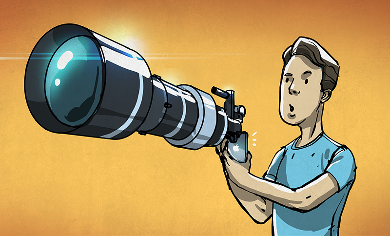
Cool, but why is the graphic a picture of a phone being used as a *telescope*?
Interesting article, the company I work for actually makes a phone stand that attaches to a microscope. Its a bit pricey but not everyone has access to a 3d printer, http://www.scientificdevice.com/microscopeplatform/
FUQ THIS GARBAGE!!!
What happened to that $1 dollar microscope?
No… I am serious. Did this upset the status quo? Or did I witness a “Gypsy took the money and ran.”
https://en.wikipedia.org/wiki/Foldscope
http://www.npr.org/sections/goatsandsoda/2014/09/03/345521442/a-1-microscope-folds-up-from-paper-and-a-lens-of-glue
http://www.wired.com/2011/03/diy-cellphone-microscope/
http://www.ted.com/talks/manu_prakash_a_50_cent_microscope_that_folds_like_origami?language=en
http://www.theatlantic.com/science/archive/2015/09/one-dollar-origami-microscope-foldscope/403156/
http://www.foldscope.com/
https://en.wikipedia.org/wiki/Foldscope
This was so called $1 dollar. Do some research. Just submitted an article 10 min ago with 5 different URLs. Go on. Tell us why $10 is better then this. Was this fake? or Just buried.
Always great to hear more microscope hacks!
Our lab designed 3D printed + laser cut sample chambers for inverted microscopes. Work great for any sample you have in aqueous solution (or whatever’s compatible with your filament) that you want to image through glass and is a helluva lot cheaper than anything we could buy.
https://github.com/PRNicovich/BenlideChambers.git
Cool article, “stole” some links for later reference… As a retribution, here are some that might be interesting?
The Flypi – a small device for microscopy and behavioural testing on invertebrates, using the picamera https://hackaday.io/project/5059-flypi
A collection of open source hardware related to science – from both academic and non-academic sources, plus there are some microscopes there – http://collections.plos.org/open-source-toolkit-hardware
cheers
could we agree on cell phone microscopy? it might be hard to believe for apple fanboys but iphone market share is only 20%…
CMOS is getting better yet 10 year old CCD digital cameras with big glass lenses still take better photos than multi-megapixel phone cameras. Zoom in on a CCD taken image and you see *pixels*. Zoom in on a CMOS taken image and you see *blur*. 2 megapixel CCD will easily beat 5+ megapixel CMOS in image quality. Sure you can pile on more sensor cells in a CMOS chip and add better lenses, but when you zoom into the image it’s still blurry. Shrinking a CMOS image in Photoshop, Gimp, Paint.NET etc can help with that.
When I want to take *good* photos I have an old Fuji FinePix Zoom. It uses XD cards. When released the max size of an XD was 512 meg. Turns out that due to some over-engineering the camera is capable of using XD cards up to 2 gigabytes. Takes half a minute to get ready with that size of card but once booted up it’ll snap high clarity pictures happily for hours.
This writeup defectively asserts that the key to taking these pictures is some modern high-resolution CCD/CMOS sensor. That could not be farther from the truth. I’ve been taking excellent high-quality digital images from my microscope (and with my camera) for more than a decade, and it has never been more or less expensive than it is now. It’s all about the optics. Quality optics produce quality images. Quality optics do not come from china. Garbage optics come from china. Some crazy high resolution CCD does not compensate for garbage optics.
Author needs to take photography 101. Lol.
Hi,
Quick question. I have been looking to buy a new microscope to use mostly as a hobby. I have searched around and read quite a few reviews. I found one scope on http://www.topmicroscopereviews.com/, i belive it was the AmScope M150C. It seems more of a professional level scope but i think it will last a long time. Do you happen to have any experience with this scope or could you recommend something that would last quite a while and not break the bank?
Thanks!