We’ve seen hundreds of ways to create your own PCBs at home. If you have a laser printer, you can put traces on a piece of copper clad board. If you have some hydrogen peroxide and acid, you can etch those traces. Don’t have either? Build a tiny mill and cut through the copper with a Dremel. Making your own PCBs at home is easy, provided your boards are made out of FR4 and copper sheets.
Printed circuit boards can be so much cooler than a piece of FR4, though. Ceramic PCBs are the height of board fabrication technology, producing a very hard board with near perfect electrical properties, high thermal conductivity, and a dielectric strength similar to mineral transformer oil. Ceramic PCBs are for electronics going to space or inside nuclear reactors.
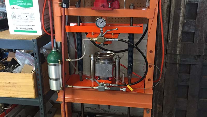
For his entry into this year’s Hackaday Prize, [Chuck] is building these space grade PCBs. Not only is he tackling the hardest challenge PCB fabrication has to offer, he’s building a machine to automate the process.
The basic process of building ceramic PCBs is to create a sheet of alumina, glass powder, and binder. This sheet is first drilled out, then silver ink is printed on top. Layers of these sheets are stacked on top of each other, and the whole stack is rammed together in a press and fired in a furnace.
Instead of making his own unfired ceramic sheets, he’s just buying it off the shelf. It costs about a dollar per square inch. This material is held down on a laser cutter/inkjet combo machine with a vacuum table. It’s just a beginning, but [Chuck] has everything he needs to start his experiments in creating truly space grade PCBs.


Seems as if this would be quite useful for a great many RF applications… Completely controlled capacitance! Very promising, this.
Why drill, couldn’t you just poke hole in th unfired sheet and take advantage of the firing process (shrinkage) to make the holes larger?
I guess green (unfired) ceramics would crack when punched. Drilling sure is the right way – not hard at all and it removes the material instead of compressing it into the surrounding parts (stressing and breaking it).
You are correct. Ceramic PCBs have very low loss and operate well into X Band.
In the past the holes were punched. If you’re doing lots of vias, the tools tend to wear. I’ll be using a layer to make microvias, if larger holes are needed, then they are essentially milled. Poking holes will distort the material. If the process is to hold a tolerance of say 1 mil then there cannot be any movement of the material. Ever. To control shrinkage something called constrained sintering is used, or materials are chosen that have low shrinkage in the X & Y axis AKA Hereaus “Zero Shrink”
I’m assuming the inking must be extremely tightly controlled. What keeps it from running during the firing process? Or oxidising?
He has an old dental furnace that can fire under a vacuum using radiant heating. Any metal will run, or even vaporise if the temperature is high enough, but if it is just liquid you can contain it just by have the right shaped substrate.
Good question: Silver melts at around 961.8 degrees C. The final sintering temp is around 850 C. As it turns out silver oxide converts to silver at high temperature.
Fun fact: you don’t need a press to do high-quality green bodies. You can use the direct coagulation casting process: http://fehu.whitequark.org/files/Documentation/Ceramics/A%20new%20direct%20coagulation%20casting%20process%20for%20alumina%20slurries.pdf, and then with a minor additive you can greatly decrease the temperature at which alumina is sintered without decreasing its density more than by a few %: http://fehu.whitequark.org/files/Documentation/Ceramics/Sintering%20of%20Alumina%20at%20Temperatures%20of%201400%C2%B0C%20and%20Below.pdf.
Thanks for the great references. Typically LTCC ceramics from commercial suppliers have a light blue color suggesting the presence of Boron AKA Gerstley borates as a flux to lower the melting temperature. An yet, at least for the compositions from the suppliers I’ve seen don’t mention Boron at all.