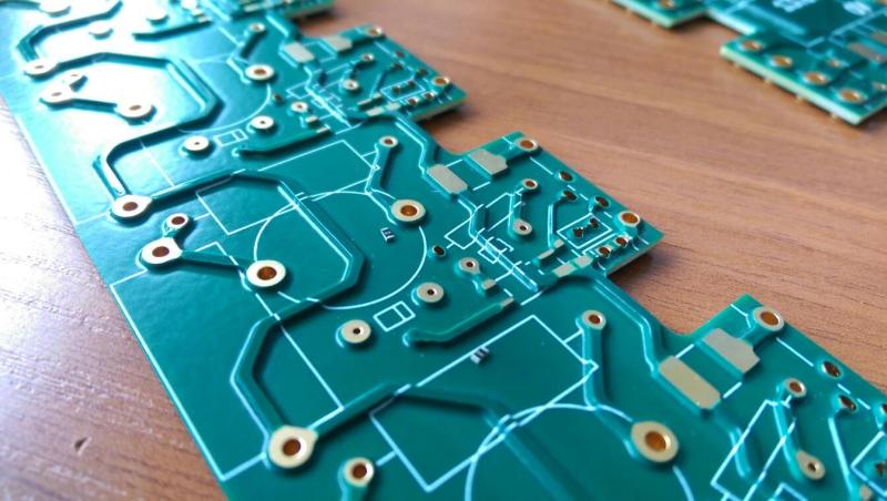
Is twenty times the copper twenty times as much fun to work with? Ask [limpkin] and follow along as he fabricates a DC/DC block for a Formula E race car on 20-oz copper PCBs.
The typical boards you order from OSH Park and the like usually come with 1-ounce copper – that’s one ounce of copper cladding per square foot of board. For those averse to Imperial units, that’s a copper layer 34 micrometers thick. [limpkin]’s Formula E control board needs to carry a lot of current, so he specified 700-micrometer thick cladding, or 20-oz per square foot. The board pictured cost $2250, so you’d figure soldering on the components would be an exotic process, but aside from preheating the board, [limpkin] took it in stride. Check out the image gallery of the session and you’ll see nothing but a couple of regular high-wattage soldering irons, with dirty tips to boot.
It’s pretty neat comparing what’s needed for power electronics versus the normal small signal stuff we usually see. We’d recommend looking at [Brian Benchoff]’s “Creating a PCB in Everything” series for design tips, but we’re not sure traditional tools will work for boards like these. And just for fun, check out the Formula E highlights video below the break to see what this build is part of.
https://www.youtube.com/watch?v=UUZ3faWp4m0
Thanks to [vinnycordeiro] for the tip.


For $2250 I would think you could just mill some copper plate and glue it down to some fr4.
Or the other way… epoxy it to fr4 and then mill it…seems like that would be easier to me.
Dip the whole thing in paint as solder mask then drill all the through holes and the mill the paint off pads. You’ve got plenty of copper to work with.
$2250? I think I would have used point-to-point wiring with whatever gauge was needed. Duh.
Weight, and vibration control. 4Tthis is after all an elite motorsport.
point to point wiring and fixing it with a dissolveable resin layer so you just dissolve it, repair and pour resin back in.
a Metcal or JBC iron would have soldered this fine without a hotplate.
I have soldered some big stuff with my metcal, but I think this would be too much for it.
This is the reason to buy a seventy year old American Beauty for 5.00 at a hamfest, the kind that has a heating shaft on it bigger around than a curling iron… Oh yeah–she’ll heat up. This board is a lovely proof of concept, but I’m with the other commenters who took one look at the price and were immediately sent brainstorming an alternative build.
Metcals can solder pennies together….
Most pennies are zinc core.
Can confirm. I’ve soldered wires to pennies before for makeshift 18650 battery contacts. I’ve also soldered brass plugs in 1″ brass Sharkbite fittings for temperature sensors in a hydronic heating system. Also soldered 4AWG (not easily) when repairing a car battery cable. MX-5000s (and MX-500s) are beasts with the right tips.
We had a power board intended to run 50A semiconductors through the power section, but containing a digital section as well, so we ended up getting 10 ounce copper on half and 1 ounce on the other half. That board was a nightmare to work with, and it cost a mint. We deeply regretted going that route. We’ve since done similar work on two ounce copper using massive, massive copper pours/planes to move the current around, rather than discrete traces, and found that far more rewarding (and in the rare case where that was still not enough, we’ve hand-soldered 14-ga bare copper wire down on top of the exposed copper plane and then sprayed the whole works with conformal coating.) If you can avoid weird custom boards, make every attempt to do so.
I’ve done that too, with copper strips doubling the heavy traces for more cross section. It’s not the fabrication nightmare that you would think at least in small runs. For us the trick involved pre-cutting and tinning copper strips to the right size and heating them to reflow temp in an oven. We’d pre-heat the board on a plate and place the hot strips on the board and immediately get it into a reflow oven.
it took a bit of tweaking to be able to do it without warping but once we dialed it in it wasn’t a problem. then we’d just conformal coat it all when we were done.
Also, it would be remiss of me if I didn’t point out that there are actually commercial products out there specifically for reinforcing high current traces. They are called PC bus bars and look like a strip of copper with pins every inch or so on one side. they stand sideways on the board and they look kinda like ridiculously long sip resistors.
That’s really useful, thanks for providing info. Is there an SMT version? Are they offered from places like digikey?
The surface mount version is just soldering stripped copper wires to the traces. Works pretty good but make sure you have a good temperature controlled soldering iron because you are putting a large mount of heat into the board and you can delaminate it.
Hmmm.. to me the obvious question is why are traces so narrow? I suppose he could have been fighting some factor that’s not obvious to me, but my first instinct in laying a power board out is wide, wide traces.
it looks like he easily has room for traces, say, three times as wide, and they could be a third the thickness while keeping the same cross section.
Traces three times as wide would provide probably maybe 2.5x more surface for cooling, and, depending on his switching frequencies, for fighting skin effect.
Like I said, I assume there’s some reason he went skinny and tall (maybe voltage separation?) but I skimmed his write up and I didn’t see it addressed directly, and I’m curious what it might be.
Still, gotta admit, damned cool.
In the reddit thread, limpkin states “the side that you’re looking at has -450V / 0 / +450V traces. The other side has 14V @ 150A and 24V @ 80A.” The other side being this: https://usercontent.irccloud-cdn.com/file/ZjnBND2U/irccloudcapture-236812244.jpg
How many of those tracks actually needed to be that heavy? Hard to see how it wouldn’t have been way cheaper to use wire to reinforce where necessary.
All of them, since this seems just made more for the show than anything else!
How is it produced? Milled board? At that thickness I would imagine etching is liable to undercut your traces.
According to the comments by the OP on Reddit, The board was made with a 2mm thick copper sheet bonded to the bare FR4. The board was then etched in the usual way. There are some pads that etched too far and the hold just has a little mound of copper around it so it’s easy enough to find them in the image.
>we’re not sure traditional tools will work for boards like these
Why not? How would the gerbers be any different from ones for 0.5 oz, 1 oz, or 2 oz boards?
My first thought also.
There is a PCB house in Queanbeyan (Australia) that uses a copper vapourization technique to build up pcb tracks to the desired thickness.
From what I recall of the process a thin blank board is etched then the plateing process only builds up the tracks – masking I believe can be applied to allow for mixed thickness tracks on one pcb.
http://www.lintek.com.au
I was thinking something along these lines must exist, or some sort of electroplating process!
Vapour phase sounds more appealing than using copper sulphate in a bath…
There’s also semi-additive fabrication: http://www.eetimes.com/author.asp?section_id=36&doc_id=1326796
Having seen a few “Wirelaid” boards from WE at the last Electronica show, I do wonder just how much current they could pass, and what the comparative price would be, if suitable for this application!
However, the tech doesn’t look like you could acheive the conventional layout style shown here with Limpkin’s board.
Worth a read though, I’m considering it for applications in place of bus bar…
http://www.we-online.com/web/en/leiterplatten/produkte_/wirelaid_/wirelaid_2.php
Design Guide
http://www.we-online.com/web/en/index.php/show/media/04_leiterplatte/2013_1/wirelaid_1/design_rules/Designguide_WIRELAID_0713_EN_Screen.pdf
Because using some 10AWG wire and bending it, soldering it over the board is sooo passe~
Or even using copper bars themselves
Considering it’s for electric racing there are probably mechanical considerations at play.
No reason for why you couldn’t use a bit of glue, or simply solder it down in more places.
Wire isn’t that heavy. Unless it is really thick, if it is long ,then is is also going to have many bonding points.
I would at least be surprised if a 10 awg cable that is soldered (tied) down properly every few centimeters were able to break loos from the forces a race car can produce. Though, I haven’t tried, so what do I know…
for $2250 you could hire someone to bend copper wire and make the tracks, then encapsulate everything in epoxy.
Too much work? solder wire to the tracks that need it, chinese welders do that all the time, and they work fine.
yeah this is probably one place where dead bug style construction would work, go one step further and use actual bus bars for anything with any significant load, one might even be able to make a drop in controller on more common PCB material.
It is not so easy. If you dip a power circuit into a hard resin to avoid vibration damage, the different thermal dilatation between materials will rip your circuit apart. The right solution is either using a thick semi-flexible conformal coating alone or a applying a flexible coating first and then potting it into a hard epoxy.
What about a 2 side board with 20 oz on one side and 2 oz on the other?
20oz? Hell, I did a 40oz as 14 layers, 12x3oz+2x2oz outer layers. Used Vicor factorized power modules and conduction-cooling. Goal was 95% efficiency from 28V and those Vicors were quite efficient. The fun thing about 40oz green 6×6.5″ PCBs is that they look just like regular boards but they weigh 12 ounces BARE. So the 16-board proto run weighed in at 12 pounds. These were 0.110″ thick. People don’t expect a 1.76″ stack of boards to weigh 12 pounds. Very easy to damage them because of the surprise factor.
Wow, that’s impressive, but for that much money I would have probably chosen some alternate route – either many more internal layers (with the same pattern) or just have a sheet of copper water cut to the individual traces and have it soldered on there.
What money? In a Formula E racecar? $2250 is chump change when working on such projects.
But LOOK at it: they even managed to get soldermask and silkscreens to conform to those ridiculous traces!
I think that in Formula E racing, $2250 is still the cheapest component on the car. :)
Dangerous Prototypes is the only hobbyist priced board house that offers 2-oz copper I know of. I was considering ordering some with both sides in parallel and wide traces for a high-current application.
OSH offers 2oz boards for the same price as 1oz, but with longer lead time
itead does 2oz too
Awesome production performance.
Regarding the layout… they are doing it wrong. (speaking as an ODM/hardware developer)
So much potential copper area wasted.
For the rest of the world, not using utter-crap units: 20oz are 566.99g and 1sqare foot is 0.0929m².
6100gsm
I think that the metric unit for PCB copper layers is microns, as in thickness. None of this mass-per-unit-area nonsense.
If anyone is curious, he posted a gallery of assembling the unit: http://imgur.com/a/s2zcN