 A few years ago, I wrote a few columns titled Making A Thing. These columns were a tutorial of sorts for several different 3D modeling programs. This column wasn’t meant to be a complete guide to modeling an object in OpenSCAD or SolidWorks, it was just step-by-step instructions on how to make one specific thing with one specific piece of software.
More than a few people in the Hackaday community found this column useful or at the very least an interesting pedagogical device. When starting out with any kind of productivity software, you don’t need to know how to do everything, you just need to know how to do the most common tasks.
Since the Making A Thing column was so popular, I felt it was time to revive this idea with another design task we often face. As you have already guessed, we’re going to be making printed circuit boards. Continuing the unique tutorial format created in the previous iteration of this column, Making a PCB will build one specific circuit in multiple EDA suites.
The Circuit
The entire concept of demonstrating how to build one thing in a specific software package necessitates a model thing. Before I even begin writing the first Making A PCB column, I need to design something that’s sufficiently complex but still relatively simple, and something that’s hopefully somewhat useful. Breakout boards are extremely simple, perhaps too much. In the course of these programs, I’ll need to demonstrate how to make a part in each specific software suite, so fewer pins are better.
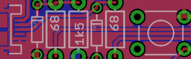
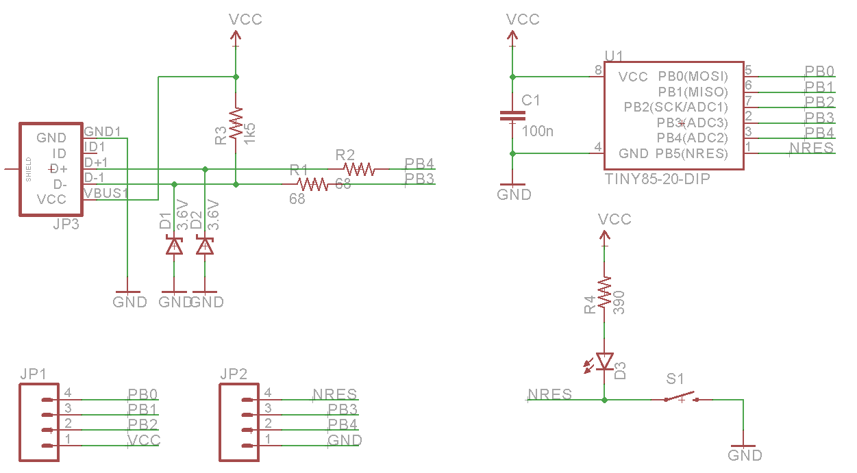
Lacking any creativity of my own, I’ve settled on a very small ATtiny85 Arduino derivative from Tim a.k.a. [cpldcpu]. Tim’s Nanite 85 is an exceptionally small Arduino-compatible board based on the ATtiny85, complete with a USB port, LED, and a few pins of I/O. It’s simple but sufficiently complex to give an introduction to a PCB design suite.
I’m not going to outright copy Tim’s Nanite 85, though. It’s much clearer if parts aren’t stacked on top of each other, and I’d like to give myself a little breathing room on the layout. I’ve redesigned the circuit of the Nanite 85 to use mostly through-hole parts on a slightly larger board. I’m calling my version the Nanite Wesley, and if you get that reference, thumbs up for you.
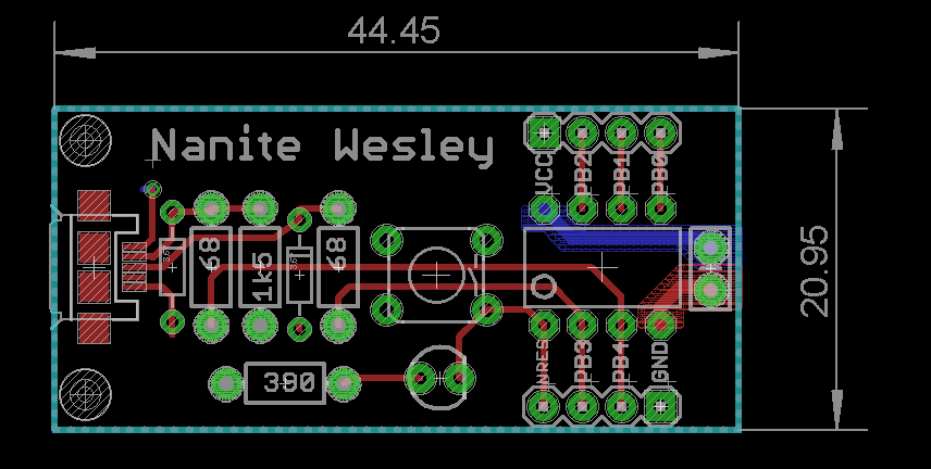
Is this how a board should be laid out? No, absolutely not. I could probably do this as a single-layer board. This is a very inefficient layout, and I like rounded corners on my boards. It’s good enough, though, and it works. This is meant to be a tutorial on how to use a PCB design package, not a tutorial on how to design a PCB. Your criticisms in this regard are noted and ignored.
What These Tutorials Will Consist Of
You cannot use a PCB design package until you know how to make a part. Yes, Eagle has wonderful libraries for almost everything you can imagine, KiCad has plenty of parts on the Internet, and if you’re using a cloud-based PCB software, almost everything will be provided for you. If you make a PCB, eventually you’ll have to make your own part, though, and each tutorial will begin with making a DIP-8 ATtiny85. Everything else on this board is a jellybean part. Either way, the process of making a part and package for a Zener is the same as making one for a microcontroller.
The next part of the tutorial will consist of schematic capture. This means placing the parts in the schematic, drawing wires between the pins and pads, and naming them. From there, it’s time to actually make a board, and this means dropping the parts down, putting traces between all the pins, doing the board outline, pouring copper, and mechanical considerations.
With the schematic and board designed, it will be time to send it off to a fab house. For Eagle and KiCad, this is easy; OSHpark accepts Eagle .brd and KiCad .pcb files, but this is cheating. We’re going to use CAM to generate real Gerber files. If you make enough PCBs, you’ll have to learn it eventually.
Caveats and Poor Design
There are a lot of things that go into making a ‘proper’ PCB, including isolation, direct traces to decoupling capacitors, making sure pixies don’t go around sharp corners and a thousand other items that won’t be discussed in these tutorials. There’s a reason I won’t be discussing this. This is a guide on how to use a PCB design tool, not how to design a PCB.
What else should I do?
As you can probably guess from the schematic above, the first PCB software I’m going to cover is Eagle. KiCad is on the list, as is Fritzing, Altium CircuitMaker, and OrCAD. In the interests of putting PCB design in a historical context, I have a copy of AutoTRAX and an old DOS machine. I’ll also be covering a few of the cloud-only design tools such as Upverter.
That’s enough software suites to get started, but as with the Making A Thing series, I’m going to be looking for suggestions from the peanut gallery. I can’t change the circuit I’m making, as that’s the entire point of this series, but I am looking for suggestions on other tools to cover. What else can I do? Want me to grab a piece of copper clad board, sticker overlays, and some photostatic film? I can do that. Are you at a web-based EDA startup, and want some free advertising? Leave a note in the comments.
Thanks to our efforts to slowly improve the backend of Hackaday, you’ll be able to access all the Making A PCB In Everything posts from the series list below.


I’ve started out using UltiBoard 6 or 7 (I think) when I studied electronics. Back then it was a DOS version but the Windows version was on the horizon. I got a student license but soon started using Windows and was looking for something that was free or low cost and runs on Windows. Somehow I can’t remember I started using CircuitMaker. I really liked the way you could draw and move objects around, very intuitive. Somehow I was under the impression that CircuitMaker wan’t updated anymore so I started using Eagle because it seemed very popular, and the huge libraries are a real boon. It took a long while to get used to the unintuitive interface but I’m now comfortable using it, especially when you setup your own keyboard shortcuts.
Something I’ve never done before and I’m looking forward to is how to prepare your design for a board fab house. I mean properly, with all the tolerances, drill holes, solder masks etc. How to export, what files are important. An actual step by step tutorial would be very helpful.
Sorry, my comment below was meant to be in response to you.
Would UltiBoard happen to be related to UltiSim/MultiSim?
That’s right! Ultiboard/ultimaker bought the company of electronics workbench, if I remember correctly, and renamed it to ultisim.
Another thing that would be interesting is a tool to get a 3D render from the PCB. I use Lightwave 3D a lot for part design including enclosures and print it using the prusa i3 3D printer. I know I can export Eagle files in dxf, load that in Illustrator, convert to EPS and import into Lightwave, but that’s a lot of work. I know that some packages have the 3D shape files already on board and the output seems pretty accurate. The most basic thing would be to have a boundingbox of each footprint, and the height, then extrude the footprint to that height. This can often help to design a case and get everything to fit in it while the input/ouput and controls are placed and mounted correctly.
I hope Autodesk will implement a 3D view and export function in Eagle and hopefully support stl and/or obj fileformat.
It would be interesting how other packages handle this type of thing. The problem is often that only the most common parts have a matching 3D shape in the library. Would it be possible to add custom 3D shapes?
Not a tutorial, some suggestions if you’re looking to learn:
Sunstone and OSH Park have downloadable Eagle DRC and CAM preset files. DRC is the design rule check. Design rules specify the clearances and other layout details, which are specific to each fab house. The Eagle CAM output dialog is where you enter specifications for gerber and drill files (what you actually send to the manufacturer). I found tearing into those and tweaking values helped me learn a lot early on. Sparkfun also had some tutorials that dig a bit into the details.
http://docs.oshpark.com/design-tools/eagle/design-rules-files/
http://docs.oshpark.com/design-tools/eagle/cam-job/
http://www.sunstone.com/pcb-resources/cad-tools/eagle
https://www.sparkfun.com/tutorials/115
I also recommend a gerber file viewer to check the files before sending them off. Gerbv works just fine.
http://gerbv.geda-project.org/
@bentwookiee: thanks a lot for the links and explanation! I’m considering using a fab house to make a more complex board that would be hard to make myself. The cost and delay usually put me off but it would make it easier if I knew how to do it succesfully in one try :)
No problem! The cost has come down considerably, but the delay is generally still there. At my last job, I would typically just use that time to finalize my BOM, order all of my parts, and get my documentation in order. We used OSH Park a lot for prototyping runs. It was invaluable as far as providing a tangible proof of concept close to what our main board house would provide, helping find issues before a product ever hit production. We also used 4 layer boards for most of our products, so DIY was almost always out of the question.
I’ve been using DesignSpark lately. Pretty good, free, package. You might add it to your list.
I am interested in the KiCad creation though. I’d like more import/export options than DesignSpark has.
I’m assuming the limitations are because of its development.
https://www.youtube.com/watch?v=JN_Y93RTdSo&list=PL5iUxv3Op2fOpVASHvcpM2O4UO0yMfKJi
That playlist might be of interest to you. It moves along similar to what Brian is planning to do and then finishes the process by ordering and populating the board right through to troubleshooting.
+1 for the request for Brian to include DesignSpark PCB in this series comparison!
I’ve only ever used KiCad. Looking forward to a back-to-back comparison with other popular packages. Also, keen to know about design file availability for the cloud-based platforms–i.e., how one can download and share them freely in the OSH spirit.
“Could someone remove this child from my bridge?”
My daughter plays out an ongoing fantasy being the First Officer of large Federation starship that is run by children.
She often beams aboard the Enterprise 1701-D (while she watching an episode) to offer helpful (NOT!) advice to Captain Picard.
I’m sure she enjoyed the episode of him trapped in the turbolift with some kids or the one when him, Guinan, and Ro was kids. I was thinking, once my skills are good enough, of building a helm system based on the one from the Enterprise so my kid can stay stuck in one place and mash touchscreen buttons to his heart’s content.
Cool and you could have buttons to cover all emergencies, like, “Rotating shield frequencies.”, “Reconfigure deflector array.”, “Send Riker to screw the female one.”
dump the warp core also seemed to be required a lot
I don’t think people realize how much work actually goes into a design… ;)
Here are a few time lapse videos of a project I am currently working on, in Altium Designer:
Schematic capture, part selection, schematic symbol, footprint, 3D model, etc…
https://youtu.be/oUnSPCgVgMk
Actual Layout:
https://youtu.be/vT8N5XV0Rc8
I never really understood why people spend time watching videos of other people playing video games. But I just spent 16 minutes watching schematic capture and board layout in time lapse. :)
Heh, they can get quite mesmerizing, but I don’t think they will be making a sport of it any time soon. ;)
Here is the whole playlist if you want to waste more time:
http://www.youtube.com/playlist?list=PLQdu_G7xyFIR29L5izNZavf4Uf8IMWuZm
Was that a discrete boost converter? What was it for?
Yes, it is a discrete boost converter.
Takes in +5V from a USB power pack and boost converts up to +12V to power the BMS in the Nissan Leaf battery pack. Then I can read out the state of all 96 “cells” and display them.
Suggestion: PCBmodE
Now that’s one I’d be very interested in seeing, mostly because it’s so counter to all other PCB-making packages.
I’m really curious to see the difference in Eagle vs KiCAD vs CircuitMaker vs UpVerter. I keep wanting to evaluate the others but end up running back to Eagle because its what I know and I’m impatient to get things running on my current projects. Super excited to for the series! Thank you Brian!
I’m really curious to see the difference in Eagle vs KiCAD vs CircuitMaker vs UpVerter. I keep wanting to evaluate the others but end up running back to Eagle because its what I know and I’m impatient to get things running on my current projects. Super excited to for the series! Thank you Brian!
I’ve been looking into easyEDA – a browser based software. It would be cool to look into that one too because the software is free and it includes a option to order pcbs directly. Looks pretty cool but it would be great to see how it compares.
I haven’t used any of this software before and this series is timely for me given that. .. I’ll stay tuned
I’m looking forward to the “in everything” coverage because I am having trouble finding an object library for mspaint.
Press Alt and Prt Sc at the same time while reading the PDF spec sheet.
You said the name, I say the meme.
“Shut up, Wesley!”
I would have thought that using t/hole for the USB would have been a priority too. For those inexperienced with SMT, that connector is a more difficult one to solder.
DigiKey do have a mini-USB t/hole connector (~$1.50 IIRC), or just use a cheap full size.
Why use double layer in such a simple board? Single layer boards are easier to manufacture at home with toner transfer method.
Take as an example similar projects like Silspark and Modder’s friend
https://cdn.hackaday.io/images/9100891457317119354.png
https://cdn.hackaday.io/images/5723011471829092321.png
Or bigger boards like Chessmate and AVeRCADE
https://cdn.hackaday.io/images/5860161449530588455.png
https://cdn.hackaday.io/images/6306581473723810453.png
Go and get your single layer boards scanned for emi.
Why would such projects worth worth so much effort, Dave?
Or you can route double layer but only use the top layer if you really really can’t fit it on the bottom layer.
Then just have the board made single layer with the bottom layer only and all the top traces are soldered in as wires.
Of course, the vias have to be large enough to fit a wire through.
I use to do it a lot. Straight lines are routed on the top layer during the design and replaced by jumpers when assembling the board.
Probably because the point is to show how to use the software, not how to etch a PCB at home. Surely readers will want to know how to use multiple layers even if they don’t always chose to do so.
I still love my DALO pen…
One thing that probably almost nobody in the “hacker-community” seems to be aware of is that there is an organization called the IPC. They have a lot of handy and well researched guidelines, like the IPC-7351 Generic Requirements for Surface Mount Design, IPC-2221A Generic Standard on Printed Board Design, IPC-2222A Sectional Design Standard for Rigid Organic Printed Boards, IPC-2152 Standard for Determining Current-Carrying Capacity in Printed Board Design… and a lot more.
I’m not saying you must always follow these guidelines to get a working board, but there is a lot of very interesting and important information in these standards, and a lot of people could learn something about how to do layouts the right way. It’s sad that that most of this information is hidden behind a paywall, but some clever searches can lead you to “free” documents floating around on the web too.
Strangely, noone has mentioned (or have I missed it?) DipTrace so far. This is easy to learn (for me, its workflow is perfectly intuitive) but rather powerful design tool. And it is modestli priced, too, as well as it has completely free version only limited to 300 pins in project, which is generally enough for a hobbyist. So I’m kinda surprised that noone here is aware of this CAD software, as it seems.
Bookmarked and commented. Really looking forward to this series, especially the KiCad post. I’m just starting to get back into hobby PCB design after 20 years. And the multitude of options is really amazing. But like everything when you have options, you need to do your homework and stick with it to become proficient at it. I’ve just started with KiCad because of the Opensource nature, but I don’t mind switching this early on if something looks like a better fit. Thanks Brian.
All those noname suites and you only 1/2 cover the important ones. Everybody who is anybody knows there are only two EDA suites in the world. There is only GEDA and that upstart KiCad.
+1 for gEDA pcb.
yes, design is important, still need prototype and verify if it works, then produce it with us, http://www.pcba-bright.com
No love for OsmondCocoa?
I’ve tried about half a dozen progs and currently settled on Diptrace
Also has a 3D viewer if you download the 3D components pack you get to see them on the board and outputs gerber and drill files.
Works from schematics or manual placement and does a good auto layout as well
Lots of libs, just about to try some arduino and raspberry pi components.
This is a whole lot of information on circuits I didn’t have before. I’m taking a computer science class in college so I’m trying to get a handle on new tech and basically the “guts” of computers. Thank you for the article, I learned a lot more about pcb!
What about an update with EasyEDA? Even if it got serious issues as Fritzing, it worths at least a small page describing it.
Can you include a tutorial of Proteus? Perhaps the more intuitive:
https://www.labcenter.com/
I have to add that Diptrace is a pretty great program. I started with eagle years ago but my AutoCAD brain could not, after three years get in the workflow groove of Eagle. So I jumped ship one night after hours of frustration. Now, 8 years later, I’m a full fleged Diptrace guy. I used the free version for about 4 years and Now I’m on the “semi-pro”? version.
The library and components take some getting used to and it’s not as powerful as some of the big guys, but I think I’m getting pretty amazing designs.
I do have a wish list – and 1st would be to get Polygon shapes in the gerbers. Right now gerbers are lines, so copper pours are hard to get into a CNC machine. Its fine for PCB fab shops, but if you want to prototype on your workbench, it’s too much work. I’ve been looking for ways around this, but every software program that makes CNC Gcode gets overwhelmed by the way the files are made.
However, the 3d renders are Amazing and being able to export a 3D step file is awesome when working on physical integration with enclosures and connectors….
Anyway – Recommended.
An update with EasyEDA appreciated.
I’ve used it and found it pretty “easy” – what are the big issues?
I don’t mean this to sound like a commercial but here are some details on a PCB artwork program that I have used since my prior go to DOS program Accel Tango PCB Series II+ won’t run well (on DOSBox) or any other modern opsys. In the end the replacement product was far superior:
If you are looking for a very easy to learn and bug free PCB program (sorry no autorouter need apply, well it does have a point to point autorouter but I never use it). I highly recommend SprintLayout 6.0. I have made probably 1000 board designs with it. Great product, great features, very quick to learn and use. Creating components is a snap. Not free but very close to free. Runs on Win7-10 and Linux under WineHQ. Video quality is amazing. Has 274-X to PCB import capability and also float the BMP for getting artwork off a printed page. Great for toner transfer. Can be used with a CNC machine to route PCB’s using MACH3 or LinuxCNC by using the free 3rd Party tool called SL2M3 by Bernard Pahl which converts the files to G-Code files to run the CNC. Cost inside the EU is 49.9 Euro outside the EU 19% less as EU has a 19% VAT. Demo versions available that don’t save or output. The Demo version can be used as a viewer. The full version installed is well under 10MB. No dongle or weird keycodes to deal with. They have a free lightweight viewer that can be used to view their CAD files directly. I have used the program recently to create some PCB’s that were make by jlcpcb.com. I had about 14 different layouts with different requirements (soldermask, ENIG and HASL leaded and un-leaded) fine pitch and through hole components. All of the boards were perfect. So if you are looking for a program that is easy to learn and use and AFAIK could take anything you want to throw at it (1 to 4 layers max) then check it out. The usual disclaimer: I don’t have any interest, financial or otherwise in the company I have just found their products to be very well done. Having used or tried (hobby and professionally) virtually every PCB package on the market (I go back to red and blue tape and Bishop Graphics puppets) including the very first PCB program (predates AutoTrax) WinTek smARTWORK ,Sprint is by far the best get the job done PCB artwork program out of the box I have used. In addition to all of this the company is very responsive to suggestions and the very rare occasion you need support they respond in a reasonable time.
https://www.electronic-software-shop.com/lng/en/electronic-software/sprint-layout-60.html?language=en