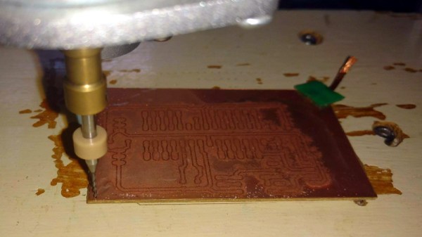
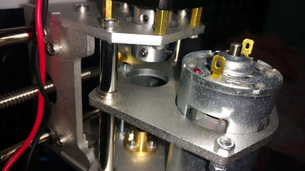
These days, if you want to build something with modern chips and components, you probably want a custom PCB. It lets you build a neat and compact project that has a certain level of tidiness and robustness that you can’t get with a breadboard or protoboard. The only problem is that ordering PCBs takes time, and it’s easy to grow tired of shipping delays when you don’t live in the shadow of the Shenzhen board houses.
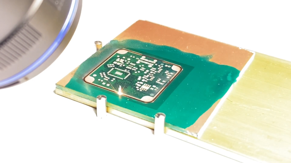
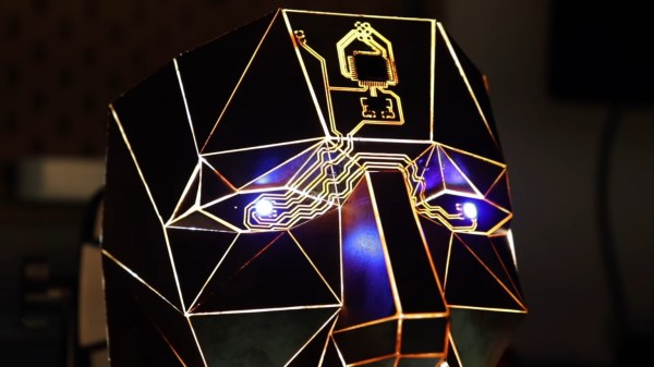
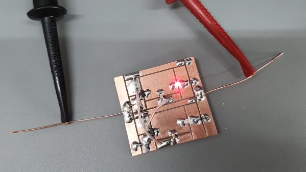
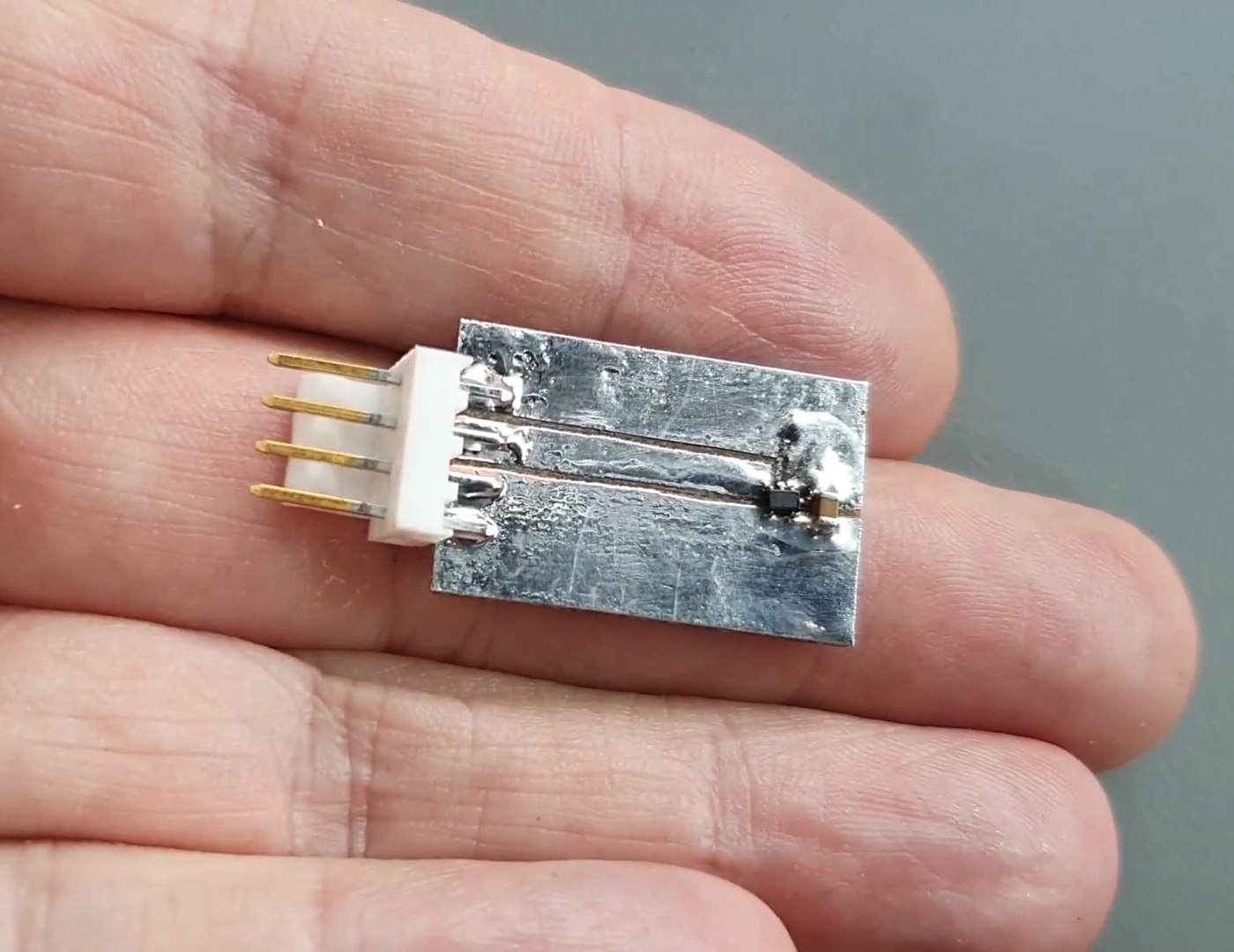
[Zach Fredin] doesn’t suffer this problem, himself. He’s whipping up high-feature PCBs at home with speed and efficiency that any maker would envy. At the 2024 Hackaday Supercon, he was kind enough to give a talk to explain the great engineering value provided by the Circuit Graver.
Continue reading “Supercon 2024: Quick High-Feature Boards With The Circuit Graver”