We bet when [devttyS0] made his latest video about RF filter design (YouTube, embedded below), he had the old saying in mind: in theory, there’s no difference between theory and practice, but in practice, there is. He starts out pointing how now modern tools will make designing and simulating any kind of filter easy, but the trick is to actually build it in real life and get the same performance. You can see the video below.
One of the culprits, of course, is we tend to design and simulate with perfect components. Wires have zero resistance, capacitance, and inductance. Inductors and capacitance have no parasitic elements in our rosy design world. Even the values of components will vary from their ideal values and may change over time.
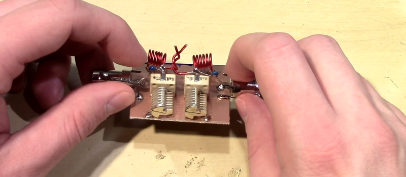
Because of that, [devttyS0] uses trimmer capacitors in the resonant part of the circuit. That way you can tune to account for circuit variances. That’s not the only practical advice offered. Need a small capacitor? Twist some wire together (a trick we’ve heard called a “gimmick capacitor”).
If you’ve been enjoying [Elliot Williams’] posts about filters, you’ll see there is a lot of difference between active audio filters and passive RF filters, although some of the ideas are the same. Watching the effect different circuit tweaks have in real time on a spectrum analyzer is very instructive. You’ll even see the effect of using shielding to separate the filter sections. If you really want to dive into RF design, you could do worse than watch these videos from [Michael Ossmann], too.


What software do you guys use to design filters? Maybe something for Mac OS X?
Qucs (analytical designs)
OpenEMS (numerical-method simulations of microstrip planar filters / transmission lines)
If your filter design requirements are typical (1-19th order filters) then there are also online calculators
e.g.
http://www.changpuak.ch/electronics/butterworth_bandpass.php
[click on filter designer (Radio, RF) and select the type of filter required]
Almost all of these online tools will spit out ideal component values, you will still need to tweak the ideal components for real world components ( E3, E6, E12, E24, E48, E96 and E192 – https://en.wikipedia.org/wiki/E-series_of_preferred_numbers ) that can actually be bought off the shelf. And then throw the tweaked values into a circuit simulator to validate that the filter still functions as expected. And maybe throw the whole circuit through a Monte Carlo analysis as well.
WinFilter – http://www.winfilter.20m.com/ … software guys make software filters :-)
Thanks for posting this. I’ve been learning about RF filters for my project: Adding 80m to a BITX40. I wrote about it at http://miscdotgeek.com/adding-80m-bitx40/ if anyone cares to read it. I’ve been bypassing the bandpass filter just for testing, but will be working to add a second switchable 80m filter to it. I bought a kit for that, but I’m interested in making my own too. I’ll be checking out these videos.
If anyone hasn’t checked out the BITX40 yet, HAD has an article on it at http://hackaday.com/2016/10/18/the-bitx-transceiver-comes-of-age/, and I’ve got a FAQ for it on my site: http://miscdotgeek.com/unofficial-bitx40-faq/
Hi Al! Just some typos mate:
1. (YouTube, embedded below)vi => (YouTube, embedded below)
2. there’s no different between theory and practice => there’s no difference between theory and practice
Cheers!
Well, we all know I don’t use vi so that must have been my editor (the human kind) ;-) The other one was me AAK (asleep at keyboard). Thanks!
Superb easy to watch and digest video, that’ll be another youtube subscription to bore my better half with when I get the remote :)
Great video, it seems almost magical when you tear open a high frequency design (like front of LNB) and nothing looks familiar. inductors are wires, capacitors are gaps, bizarre shapes are filters.
That is when you start to realize that electronic components are really all the same stuff, just different ratios. An inductor is also a resistor and capacitor. A capacitor is a resistor and inductor, and so on.. Really just different ratios of various materials. Entire high-order RF filters can be made with pcb dielectric and copper. Watching a FDTD EM simulation playback of E-fields can give you a better feel for how these waves of various lengths travel, get trapped, reflect as they move through 3-d structures of copper and dielectric (those bizarre shapes you mentioned). If you play around with these tools long enough, you will never think about electronic components the same way again.
Qucs can do simulation of distributed-element structures such as microstrip filters, if you’re looking for a no-cost or low-cost solution.
And there’s always the tinfoil-and-cardboard approach.
http://blog.svenbrauch.de/2013/01/19/rf-microstrip-breadboard/
I wonder if there’s some way to form coils by feeding wire through a 3D printer’s extruder.
Excellent video. Keep them coming!
I would like to make two comments:
(1) It may be a good idea to solder the variable capacitors so that the adjustment screw is grounded. That way, the metal of the tuning tool you show in the video will cause less drift.
(2) Filters and matching circuits, be they of the distributed- or lumped-element variety (such is the one shown here), involve series or parallel resonators. As you know, in a parallel LC circuit, the circulating reactive current can exceed the current seen by the generator or the load by the quality factor. Same for the voltage in a series LC resonator. Although those reactive currents/voltages do not appear at the generator or load (they just basically slosh back and forth between the reactive elements), they may cause losses and other problems. Therefore, it is very essential that the ESR of the capacitors in a parallel LC resonator be low enough; otherwise, the ESR of the capacitors will cause losses and lower the Q. (ATC has nice application note on this; it was written before my time, in the 1970s, but it is still available.) Similarly, in a series LC resonator which is part of a filter and/or impedance-matching circuit, make sure the capacitors can withstand the resulting reactive voltages (which appear between intermediate circuit nodes and are “invisible” to the generator or the load). The resulting reactive voltages in a series LC resonator (which may be part of a filter and/or impedance-matching circuit) may eat small surface-mount capacitors, which may be rated to only 25V, even for moderate Qs! I know because I’ve been burned by this subtle detail. So, always, always, always check the voltages at/between intermediate nodes and the currents through intermediate loops with an analog simulator to make sure that the circuit elements can safely withstand them. Similar considerations apply if the filter/matching circuit employs distributed elements (e.g. cavities), but with added complications resulting from the 3d distributions of the associated fields. For example, metal surfaces which are sharper (have more curvature) may experience higher electric fields, which may render the volume around them more prone to breakdown. In the case of distributed elements, then, 3d electromagnetic simulation should be used to check the fields in intermediate structures.