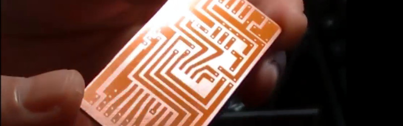
Most people who have dabbled in the world of electronic construction will be familiar in some form with the process of producing a printed circuit board by exposing a UV sensitive coating through a transparent mask, before moving on to etching. Older readers will have created their masks by hand with crêpe paper tape on acetate, while perhaps younger ones started by laser-printing from their CAD package.
How about a refinement of the process, one which does away with the acetate mask entirely? [Ionel Ciobanuc] may have the answer, in the form of an exposure through an LCD screen. The video below the break shows how it’s done, starting with a (probably a bit too lengthy) sequence on applying the photo-resist coating to the board, and then sitting LCD on top of UV lamp with the board positioned at the top of the pile.
It’s an interesting demonstration, and one that certainly removes a step in the process of PCB creation as it brings the pattern direct from computer to board without an intermediate. Whether or not it’s worth the expenditure on an LCD is up to you, after all a sheet of acetate is pretty cheap and if you already have a laser printer you’re good to go. We’re curious to know whether or not any plastic components in the LCD itself might be damaged by long-term exposure to intense UV light.
If you haven’t yet made a PCB using toner transfer, take a look at our handy guide.
Thanks [Setvir] for the tip.


About half way through, I felt like paying OHSPark to stop this insanity. So much work!
on the other hand, if you need a custom PCB IMMEDIATELY, then this is quicker than OSHpark.
I can see the pro: less waste material, no cleaning PCB up afterward. Con: LCD resolution limitation (do we have LCD capable of 600dpi?) and whether LCD can survive repeated Uv exposure.
Yes we do, not desktop ones but if you’re doing a small intricate board you can use a mobile phone display. They’re commonly used for homemade higher-than-full-hd projectors.
I would love to see a pointer to a project like that, given that these displays pretty much all use MIPI-DSI interfaces with zero documentation publicly available.
MIPI can be done (even though it is an enormous PITA of a protocol), there is some unofficial documentation out there, but unless you have the values for the hundreds of registers that have to be initialized before the display does anything, you have at best an expensive doorstop.
And you still need an FPGA or a SoC with a high speed interface to drive these.
I think the only exception were the iPad Mini screens that actually use an embedded DisplayPort interface and there were some projects making an interface board for these.
Why redesign the controller? The phone itself can control its display, and it’s easy to control a phone.
Well, good luck trying to keep it working with the phone motherboard all the while you are replacing the backlight with UV light and planting it against a PCB blank. I guess you haven’t tried something like that before, have you?
You mean like this one, at 4:50,
https://www.youtube.com/watch?v=QSPjGAaqbFM#t=04m50s
or like this one, at 7:45?
https://www.youtube.com/watch?v=IxAZl0q_tlE#t=07m45s
Might be hard to peel off the backlight spreader without damaging the LCD, but yeah the assembly is just connected through some wires and a connector to the PCB so if you manage to do that removal the rest isn’t hard.
Those layers are glued though, and you don’t want to damage the LCD/traces in the process.
The STM32F7 parts have a MIPI interface, though you’re still stuck with the hundreds of undocumented registers problem.
Yeah, MIPI isn’t the worst part, even though the official documentation is available only to the MIPI Aliance members under an NDA (and big $$$). There is enough information about it in public to implement an interface, if required. The undocumented displays are the main showstopper.
Not sure how to post a link on here, but on aliexpress you can find replacement lcds for the Wanhao Duplicator 7. They have a daughterboard with 5v and hdmi that runs a 5.5 inch screen 1440k resolution. Used for resin based 3d printers using 405-415nm light.
have you seen this? https://www.youtube.com/watch?v=7TedIzmguP0
this? https://hackaday.com/2014/08/19/a-mipi-dsi-display-shieldhdmi-adapter/
I don’t know about modern color LCD’s but the older monochromatic LCD’s suffer badly with exposure to UV.
I would be tempted to modify a VGA LCD monitor to try this as it could potentially eliminate a lot of registration issues for double sided boards but at the expense of resolution.
Currently I use the toner transfer method which gets me down to 5mil traces and 5 to 7 mil clearance and I would have to check the dot pitch of a monitor to see if that is doable with a ()VGA LCD monitor.
Double sided registration is still a problem that I haven’t completely solved with Toner Transfer.
Agreed. LCDs don’t like UV. The more modern LCDs have higher quality UV blocking coatings on the glass to prevent damage that also blocks the UV from passing through the LCD.
Don’t expect this to work long and the more you use it the darker the LCD will get.
So instead of an LCD we need an OLED display that has UV LED instead of RGB :)
So go ahead fabs, take our idea and start churning out those UVOLED displays.
the photo-resist used in this article doesn’t need UV it’s quite happy to work with fluorescent lights with longer exposure times.
Another thought: How about a e-paper display? Can you remove the background and get a transparent deal? And is that UV resistant? After all, you don’t need a speedy display for PCB exposure.
You can’t make an e-paper display transparent that I know of. The ink itself is reflective and moves (flips or sinks) to create the effect.
Though you might be on to something, namely reflecting UV off of an e-paper screen and projecting it onto a PCB. The problems may include UV damaging the ink, focus, bleed… But interesting to think about.
Nice solution.
But thinking about it, they now have those lighted e-ink displays, so what if those LED were replaced with UV LED? I wonder how dark you could keep the dark elements.
It are LED right? or is it high-voltage luminescence type stuff? And does that come in an UV variant?
Anyway if you are a reader who experiments with e-ink let us know and do some test maybe.
Pillage a rotten fruit device for its “retina” display and finally put part of it to good use.
The tablets even supposedly uses a embedded version of displayport, and since you’d be gutting the original backlight anyway so you can use a UV light source, you’d only have to focus on designing a DP passthrough adapter board and power supply for the control board.
Adafruit has a driver board available for the iPad 3/4 screen:
https://www.adafruit.com/product/1716
well you can pay adafruit or buy 2 of the the original boards from abusemark (http://abusemark.com/store/index.php?main_page=product_info&cPath=3&products_id=53&zenid=7fbonmfbpi758dli2gaepva9n0) for the same money ;)
If something like 400nm are short enough for good exposure, you can recreate a backlight with this LEDs
DisplayPort speeds for even the lowest resolution LC/AMLED/OLED glass matrix displays can just not work because of a 0.01mm difference in conductor length… Unless terminated well to compensate… unless the difference between the bidirectional channel and the video data streaming lanes are off:
Experience:
Got an eDP display to finally be recognized and the OS auto set-up an extended monitor to a blank white display, put it back on the test laptop base and the display shows fine.
I wouldn’t worry too much about the UV – there is no need to use something like a germicide lamp with strong (and cancer-producing) UV. UV LEDs are pretty sufficient and faster to expose the photoresist than UV tubes anyway. The 30 or so seconds of weak UVA light from those shouldn’t degrade the plastics too much.
I would be more worried about the display actually blocking the UV light – if the display was designed to operate with a CCFL backlight, it may have an UV filter already.
The resist that I used to use (POSITIV something) can be exposed with regular CFL “energy saving” bulbs without any problems, though exposure times were long. I’m pretty sure I could just put the phone upside down on it with same result. More worried about the blur.
Try the UV leds – cheaply available online and they expose the common resists in like 20-30 seconds. Plus no need to deal with mains/high voltage and no risk of breaking a tube. I have used them with good success using the dry film resist.
What about those halloween “black light” bulbs that will be in plentiful supply at the moment?
You could use the old photography standby: the reducer. Just use a lens to shrink the LCDs image down to the size of your board, projector style. As a bonus, it concentrates the light, so you don’t need as powerful a UV source to get the job done.
That’s exactly what I was thinking. A lens solves both problems. You could really get some fine detail in those traces with a big ol’ LCD monitor and a reducer.
Did you actually calculate how big lens you would need to reduce from a common 4k monitor/TV panel? That would need a setup as big as a room, with huge heavy lens and powerful light source. Moreover, you wouldn’t be able to use a single lens because of distortion, the reducer uses a complex setup similar to a photographic camera lens to minimize this.
That isn’t really a viable method, IMO.
Fresnel?
As a malus, glass absorbs UV pretty well if it is not selectively mixed for UV photography lenses. And focussing is not trivial because the chromatic aberration for UV (and IR) wavelengths is pretty different from the visible range of the spectrum. Hacking meets engineering and science… ;)
What a brilliant idea!
Interesting. This process eliminates the acetate and printer but requires an additional chemical, the photo-polymer. Chemical toxicity, disposability and availability are all big problems for me. Assuming those problems can be dealt with, will an old 17″ monitor laid flat work? Also, I must have missed the UV light thing. Nothing in this report indicated that it was even required. Why can’t the LCD’s original backlight work? Not enough UV? Can the LEDs be changed for UV types?
The photo resists used in this article can be used with fluorescent light so it would work with a LCD monitor of the CF back-light type but it’s unknown if it would work with an LED LCD monitor.
Dot pitches more relate to the age of the monitor than the size. You will probably get the same dot pitch from different sizes of monitor from the same era. More recent monitors have a higher dot pitch so the now very old 4:3 aspect ratio 17″ monitors are probably not that good. You want 300DPI to 600DPI for very fine featured PCB’s but older monitors may be OK for thick featured PCB’s.
You may need to make some modifications to get the photo-resist closer to the image. It may be that thin flexible laptop screens are better than monitors that have relatively thick glass.
I wonder if that would work by taking the guts out of a computer monitor remove the backlight and diffuser etc.
The process might be worth playing with as I’m finding obtaining laser printer transparency film difficult and expensive to obtain.
you don’t have to use transparency paper. I use tracing paper, a 1200dpi second hand hp laser printer and some “density toner” spray(http://www.kruse.it/en/products/chemical-consumables/mat-laser-film-toner/density-toner/) after printing. Works fine for 6/6 mil traces but i do use the expensive pre-coated bungard PCB blanks.
I have all but the daylight cure resin to do this with, so where on earth in the UK can I get this or something just as good? I’ve tried spray resist and resist pre coated boards before but the results were rubbish! So I settled with Press n Peel which was much better (TQFP 100 etch fine) although I still get a 25% failure rate. This setup with a decent LCD screen would be awesome and much less painful for me. So, anyone got any idea’s about the resin???
Thanks, Dan
What about this to try it out? https://www.amazon.co.uk/CRYSTAL-REPAIR-REPAIRING-FURNITURE-PURPOSE/dp/B01D3JK8II/ref=sr_1_1?ie=UTF8&qid=1508146076&sr=8-1&keywords=uv+cure+resin
I’ve tried the tracing paper method and it wasn’t as good as press n peel for me plus I want to get away from using a laser printer. Direct application would make double sided boards a lot easier than trying to align two acetate sheets and not damaging the toner already transferred onto the opposite side when applying the next transfer.
Plus it would be great to see the results ;)
Why would you bother going through all that hassle when a laser print on tracing paper works just fine, gives better resolution and a larger print area
Because you still have waste paper afterward and you’d need to clean PCB before you can solder.
Obtaining the laser printer is for me, not cheap, nor simple, but maybe easier than obtaining chemicals.
E.g. to put a unique ID on each PCB.
1337 points to the 1st person to convert an old photostat machine or maybe a polaroid camera into an LCD PCB printer.
I just did some quick math.
I measured my laptop wide screen which turns out to be 13″ x 9″ DOH! and has a res of 1680 x 945.
This gives a dot pitch of 129DPI and a the smallest trace width of 7.7mil and other trace widths would have to be multiples like 15mil and 23mil.
I think I will stick to my 600DPI laser prints and toner transfer unless there are better monitors with a decent work area and resolution.
Though, perhaps the inconvenience may suite some people and double sided registration would be much easier.
I’ve got a tablet PC sitting around collecting dust ever since I fried that rare version of a Realtek codec it had…
The thing contains a 16:10 screen like a REAL PC of any sort should have.
With the resolution of 1200×1920… at 8″ (OK.. It is a sideways screen, however think of the Thinkpad 8 or the Hudl 2: Same screen in both BTW). And yes: “I can still see the pixels”^(TM)
Am I correctly guessing that such a screen should yield a decent DPI etch-mask?
OK… just found a calculator… Number is rounded off to 300DPI on said screen… yet laser printers apparently can achieve 1200DPI
w00t, that’s the resolution of a pretty good dot matrix! :-D
That’s doable. It gives you traces of about 6.6mil and about 10mill (one pxl would be 3.3mill which wont etch).
I do 5 mill traces at 600DPI with a laser you don’t often need to go below 7mill so that display is in the sweet spot at 6.6mil minimum.
It would be nice if some film could be used that would react to the visible blue and violet light that an LCD backlight can normally provide. Then one could just use a phone, tablet, or monitor to expose a PCB without needing to hack in a UV light source. Even if it took fairly long exposure times, that would be extremely convenient for a quick prototype…
Try some…. https://en.wikipedia.org/wiki/Photographic_hypersensitization ???
If you made it with both red an UV backlight sources, and drilled the holes beforehand, you could display the hole locations in red and line up the PCB, without exposing it. This would make double-sided board alignment much easier.
pretty fantastic idea!
theoretically it shouldn’t break down under UV (and be pretty decent at blocking) given most auto-darken welding helmets are just a full screen LCD on a trigger circuit (a little more basic since they just darken the whole LCD at the time of the arc)
I might have to give this one a go
I’ve done sometinhg similar with a projector. It is capable of producing a sharp image the size of a post card. When you’ve got the scaling right, the resolution is enough for most projects.
“WHY NOT EXPOSE YOUR PCBS THROUGH AN LCD?”
Because UV breaks liquid crystals and the plastics used in the screens. End of discussion.
Just slather it with factor 50 banana boat, she’ll be right.
If you go to the chanel you will see that he uses a diy SLA 3d printer bed to create the pcb. On another video on his channel he actually uses pre sensitised pcb as an easier alternative than the uv liquid.
He also has some videos of removing the led backlight and securing the lcd to glass. Not recomended for sensitive viewers. ????
I’m surprised to hear people still use acetate. Acetate is not as effective as regular printer paper if the PCB file is output on a laser printer. Laser printers tend to print inconsistently on acetate, but print very well on paper. UV light passes through the paper excellently so you get a sharper image on your treated PCB. I have been using paper for at least 15 years. Prior to that I used acetate with variable results.
Sounds like you’ve been lucky with your paper. Some presentation and high density papers will have flourescing bleaches in to look brighter in normal light or may have titanium dioxide or zinc oxide in the clay gloss finishing to be all white and shiny.
Interesting that no one mentioned DLP tech…
get some gloves man, resin is a serious skin sensitivity risk.
So’s all the crap they make gloves with… well I react to 2 of them and not resin.
Have a look at this 4k UV display:
https://de.aliexpress.com/item/1005005870981128.html
Did you see the UV LCD screens offered on Ali Express?
https://www.aliexpress.com/item/1005005870981128.html