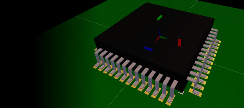
The hardest part of any PCB design is adding parts and components. You shouldn’t use random part libraries, and creating your own part libraries is just a pain. Why have we endured this pain for so long, especially considering that most components follow a standard? Add in the fact that 3D modeling and rendering a board in a mechanical CAD tool is now a thing, making creating your own part libraries even more involved.
To solve this problem, Autodesk has introduced library.io, a tool to parametrically generate component footprints for Eagle and 3D models for Fusion360. Given that most parts follow a standard — QFP, TO-, DFN, or SOT23 — this is now the easiest way to create a new part in Eagle with its own 3D model that allows you to bring it into mechanical CAD tools.
An overview parametric parts generation is written up on the Autodesk forums, and covers what is possible with this new tool. There are actually two distinct versions, one is a web-based app that allows you to create packages and footprints parametrically in your browser and export them as a library. The other version of the tool is integrated with Eagle and allows you to create a new component parametrically from within Eagle.
This is a far cry from the standard method of creating new footprints. Instead of toiling over a datasheet and dropping correctly sized pads onto a grid, creating a new parametric footprint is as easy as copying a few numbers. In addition to the new parametric design feature, there’s a new tool in Eagle that does away with placing and naming pins for symbols. Now you can simply cut and paste a list of pins from the datasheet.
It should be noted that everything created with the library.io tool can be downloaded and used offline. Combine that with the recent news that KiCad can now ingest Eagle board and schematic files, and you have a way to create parametric footprints in everyone’s favorite Open Source PCB tool as well.


Sounds interesting but I would not depend on it being around forever. Using anything from autodesk is dealing with the devil.
I concur – can we all just agree to stop posting Eagle stories until Autodesk sells them to a better steward or kills it entirely?
Hackaday has bought stock in eagle/ autotesk it seems.
This stuf is also not new. Parametric moddeling has ben around for ages and it’s slowly getting more mature.
Take for example FreeCad. The parametric plugin for fasteners let’s you easily specify length & diameter of a bolt and it draw’s it for you.
KiCad’s pcb components for IC’s which come in different sizes are also very likely script generated.
KiCad’s database is good enough that “adding parts and components” is definately not the hardest path of a pcb design. Optimal component placement & trace routing are far more difficult & time consuming problems.
Also Drawing some footpads for the pcb is a breeze. Especially with the Component Wizards and array functions for foodpads. A3D model is nice, but hardly ever very usefull.
When thinking about it more:
Drawing 3D shapes should not be offloaded to a PCB designer at all. In these modern times I expect more & more to have downloadable 3D shapes from the manufacturers (or sellers), just like the SPiCe models and the software libraries/ examples from uC manufacrurers.
The manufacturers already have the best detailed 3D cad designs of all the parts they make. Just put them on the web.
Master McCarr is also putting 3D models on the web of (almost?) everything they sell. Why would a PCB / electronics engineer be bothered with the 3d design of a chip?
Kicad part generators have been around for quite a while:
http://kicad.rohrbacher.net/quicklib.php
https://pypi.python.org/pypi/kipart
https://github.com/boseji/Kicad-tools/tree/master/libgen
https://madparts.org/ (tutorial: http://joost.damad.be/2013/12/using-madparts-for-making-electronics.html )
Eagle is finally catching up …
Just a hunch, but I bet library.io has a better UX than a hodgepodge of Python scripts. And I say that as a member of the KiCad library maintainers team.
From what I’ve seen from Autodesk that is a very risky assumption.
KiCad Librarian by compuphase is fairly good for the limited templates it has. I use it a fair bit to get me started,
https://www.compuphase.com/electronics/kicadlibrarian_en.htm
Windows app though, no python madness.What’s that? You don’t run windows? Ah well. Your loss. I just use windows and Linux in parallel and pick the best tools on each. Life is good.
It is supposed to work on Linux as well, but probably requires compiling from source. I’m in the process of sorting out dependencies to do so right now.
I use it in Linux all the time. They just don’t provide a pre-built binary.
It’s an amazing bit of software and desperately needs to be merged with or reimplemented in KiCad itself.
The only part of this that KiCad doesn’t have is nice footprint generation. But the stuff you posted handles that, as should KiCad Librarian posted above.
With respect to the main focus of the article, KiCad has long had a parametric footprint wizard. Besides, for the vast majority of parts making a footprint is unnecessary as you can use almost any standard footprint easily (a major advantage of KiCad’s separation of symbols and footprints).
With eagle is it long possible to auto generate part using the ‘make-symbol-device-package-bsdl.ulp’ This file is around since 2011, so I guess it is the other way around :) However it is not cloud based..
Lets hope the footprints are somewhat checked or guaranteed. The problem with ‘unknown sources’ you don’t know how usable the part is and it takes about the same amount of time to check as to make it yourself. I once scraped GitHub for eagle parts and it come up with lots of approximately the same footprints but minor differences. Hard to judge if it is usable. Also it depend how the PCB will be manufactured; will it be handsoldered (larger pads) or machinemade (small pads).
I can’t remember the last time I manually placed pads in eagle to create a part layout… I usually just borrow an existing package from another library, and make a new schematic symbol.
Was there one for a rectangle TQFP? I had an uncommon 64-pin IC that was 13 pins by 19 pins rather than the more common 16×16. Never found one and it took me awhile to make one from scratch that was correctly aligned with the actual chip. I never finished that part, just had the footprint for PCB and 64 pins, no label or anything else.
I’ve been spoiled by Altium, when eagle catches up to Altium (minus the content crashing and memory issues) I’ll go back.
I just started using Altium and it seems to me it’s an absolute usability train wreck. Nothing makes sense at all. It seems very much like someone just added layer after layer of menus and panels every time a new feature was added. It makes no sense to me that I have to have 5 panels open to tell what’s going on. I have to say I don’t enjoy it at all.
That’s like every EDA tool, though.
I know right? Every time we have an EDA article there are comments on how “package X is a usability nightmare”.
Making a full-featured EDA tool that lets you do everything in a simple manner is probably intractably hard. Simple to use EDA tools invariably fail to give you all the tools needed to successfully realise the most complicated designs.
In the end, you pick a package and you learn it’s idiosyncrasies, and then you’re productive. No matter which one it is. The interface is only a temporary hindrance.
I’m waiting for the package that comes in a box shaped like a kitchen sink.
That’s a fitting yet unintended description of both AutoCAD and Eagle.
I don’t know about altium though.
I’ve used EAGLE for about 7 years now. Altium is much much worse, in my opinion.
Would probably seem exactly the same if you’d been using Altium for that long and were switching to Eagle. Which I believe is the intent of both replies to you.
As for me, I use KiCad, and like it.
I dunno. I’ve used Cadence a tiny bit and find it pretty much on par with Eagle and Altlium is still way worse. I get what you’re saying – we adapt to what we use regularly. However, I’m saying that Altium may be powerful but it is more complicated than anything I’ve ever seen. That complication feels totally unnecessary.
Finaly! It was alwayssuch an hassle to create part for eagle pcb and I could never understand why it was that way.
I used to do this with excel and export a csv to import into Eagle (many versions ago). Seems like it always needed some final tweaks. The big issue I ran into was that different manufactures used differing coordinate references. Some referenced all dimensions from the center of the part or pad, others from one corner and still others used various combinations on the same part.
You are amazing! How far did you get?
It was good enough for my own use. It took a few back and forth tries to get it right. I used the concatenate() function to combine dimensions and text for each line in script file that Eagle could read import. This was many years ago, so I don’t know if it’s even an option any longer.
” Instead of toiling over a datasheet and dropping correctly sized pads onto a grid, creating a new parametric footprint is as easy as copying a few numbers. ”
I still think this is something the manufacturers should do. Just like with mechanical parts, like screws and fasteners.
This exactly. For a tiny part of their marketing budget, manufacturers could produce footprints, electrical, and thermal models. Produced in a standard format they could be integrated into a global library that would greatly reduce time wasted by countless engineers redesigning the same thing.
ultralibrarian
I don’t remember having to design “standard” packages in Eagle. Most of them were pre-drawn in the ref-packages library and were just a copy-paste away.
We have been going about this all wrong for years. We should demand that any IC manuf. that sells a part create the PCB and schematic symbol, and that is in some open standardized format that all app can then use.
+1
It’s not just as simple as “one canonical footprint per part”, though. There are specific standards for pad sizing that vary based on the manufacturer capabilities, and a lot of complicated calculations to go from say “QFP-64” to an acceptable footprint in the standard required by the manufacturer.
So of course companies have evolved to fill this space. You buy a license for their tool and they do the part generation and library management for you. They pay manufacturers for access to their part data and onsell that to the users. That provides them with a strong incentive to not provide that data publicly.
That’s where laws come in. They can strongarm them to provide the data.
What in our current system of capitalism makes you believe that would ever happen?
Welcome to the world of Ultra Librarian, i guess. The tools exist, but so far not many adopted them. TI is at the front of it for now i guess.
The Ultra Librarian Reader is a free tool that lets you convert the neutral file into CAD specific formats. they support 20 different packages now, fom KiCAD and Eagle all the way to Altium, Mentor, Zuken …
Nothing new here,nor very usefull. Mentor has LP-wizard ,which is a similar tool.
At first sight these tools look very handy, but as soon as you have a pretty solid library with parts,
you’ll see it’s of no use.
Why? We already have all the DFN’s QFP’s 0603’s and the like already in the library.
New part creation ? connectors ,inductors,transformers, common mode chokes.
And that’s just where these tools are of no help at all.
On the contrary I would say. You’d better put effort in mastering your PCB software,especially the library creation.
rather than trying to figure out what all parameters do exactly in those silly tools.
Can anybody layout circuit cards without a “tool”? What if you just got a logic diagram , no pull ups or decoupling caps or
no pins assigned.you put the board power supply parts down +5,-5 filter caps etc. Just something to think about.
About 20 years ago, when i learned electronics, we already had the tools available (Protel 98 in my case). But we still had to make our first boards by hand, just to learn the old ways. For the power supply e used special tape for the tracks and stickers for the pads and drew the (mirrored) layout on a transparent foil. This was then uv exposed and etched into a PCB.
The second board we did was a 4-digit counter circuit with 7-segment display we completely wire wrapped. I guess that would qualify as making a circuit board without software tools too.
Nah. I’m still not buying it.
This whole article has nothing to do with any kind of “hack” and it deafinately is not related anymore to the “hacker community” since eagle has been bought by the dark side.
If you want some news in the hackers related PCB design word: KiCad has been long awaited and rumors of it’s coming are getting stronger and stronger. No hint yet on the KiCad site, but this looks promising:
https://bugs.debian.org/cgi-bin/bugreport.cgi?bug=891286
[quote]
Changes:
kicad (5.0.0~rc1+dfsg1-1) experimental; urgency=medium. [/quote]
I was a bit apprehensive of posting this here.
Please let all the volunteers who work on the progress of Open Source SW just do their work without them having to read mails about questions of new releases. It will only slow their progress down.
KiCad had a Widget for footprints since at least 3 year ago…
There are also scripts for building footprints used already to create the KiCad fp library
https://github.com/pointhi/kicad-footprint-generator
For 3D models there are already scripts that have been used to build the actual extensive 3D model KiCad library…
Also those scripts are available since almost 3 years.
https://hackaday.io/project/7926-kicad-stepup-script-hacks-mcad-world
(search the article for ‘3D parametric models library’)
ATM there are more than 4 thousand 3D models available for KiCad users, mostly script generated.
KiCad’s librarians made a lot of good work…
I can’t stand this “making parts/footprints is a pain” moaning. If making custom parts and footprints for them is the hardest part of your electronics design workflow, then start working on something more complicated than a 555 LED blinker. Having been a professional design engineer for years I take pride in making my own libraries which I know are 100% correct and working. Most PCB design packages already have wizards which take care of generating decals and footprints so the news about this Autodesk app is certainly nothing new (as others already pointed out). If you’re not making a 500-ball BGA package then making new parts shouldn’t take very long at all. You will get used to it (and even start to enjoy it!) after a while.