Proper Routing Makes For Many Happy Return Paths

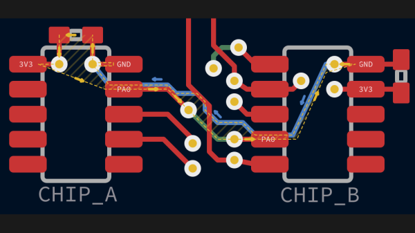
Here’s a question for you: when your PCB has a ground plane layer, where do return signals flow? It seems like a trick question, but as [Kristof Mulier] explains, there’s more to return path routing (alternate link in case you run into a paywall) than just doing a copper pour and calling it a day.

Like so many other things in life, the answer to the above question is “it depends,” and as [Kristof] ably demonstrates in this concise article, the return path for a signal largely depends on its frequency. He begins by explaining current loop areas and how they factor into the tendency for a circuit to both emit and be susceptible to electromagnetic noise. The bigger the loop area, the worse things can get from a noise perspective. At low frequencies, return signals will tend to take the shortest possible path, which can result in large current loop areas if you’re not careful. At higher frequencies, though, signals will tend to follow the path of minimal energy instead, which generally ends up being similar to the signal trace, even if it has a huge ground plane to flow through.

Since high-frequency signals naturally follow a path through the ground plane that minimizes the current loop, that means the problem takes care of itself, right? It would, except that we have a habit of putting all kinds of gaps in the way, from ground plane vias to isolation slots. [Kristof] argues that this can result in return paths that wiggle around these features, increasing the current loop area to the point where problems creep in. His solution? Route all your signal return paths. Even if you know that the return traces are going to get incorporated into a pour, the act of intentionally routing them will help minimize the current loop area. It’s brilliantly counterintuitive.

This is the first time we’ve seen the topic of high-frequency return paths tackled. This succinct demonstration shows exactly how return path obstructions can cause unexpected results.

Thanks to [Marius Heier] for the tip.

A 555-Shaped Discrete Component 555

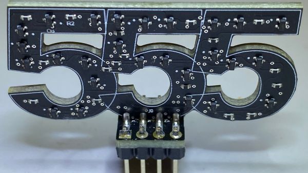
While the “should have used a 555” meme is strong around these parts, we absolutely agree with [Kelvin Brammer]’s decision to make this 555-shaped plug-in replacement for the 555 timer chip using discrete parts, rather than just a boring old chip.

As [Kelvin] relates, this project started a while back as an attempt to both learn EDA and teach students about the inner workings of the venerable timer chip. The result was a 555-equivalent circuit on a through-hole PCB, with the components nicely laid out into the IC’s functional blocks. As a bonus, the PCB was attached to an 8-pin header which could be plugged right in as a direct replacement for the chip.

Fast forward a few years, and [Kelvin] needed to learn yet another EDA package; what better way than to repeat the 555 project? It was also a good time to step into SMD design, as well as add a little zazzle. While the updated circuit isn’t as illustrative of the internal arrangement of the 555, the visual celebration of the “triple nickel” is more than worth it. And, just like the earlier version, this one has a header so you can just plug and chug — with style.

Want to know how the 555 came to be? We’ve covered that. You can also look at some basic 555 circuits to put your 555-shaped 555 to work. We’ve even seen a vacuum tube 555 if that’s more your thing.

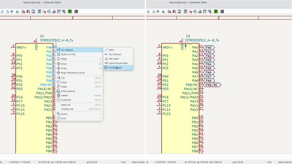
An image showing the new KiCad feature that allows you to easily generate schematic labels from IC symbol pin names

KiCad 8 Makes Your Life Better Without Caveats

A few days ago, KiCad 8 was released, and it’s a straight upgrade to any PCB designer’s quality of life. There’s a blog post as usual, and, this year, there’s also a FOSDEM talk from [Wayne Stambaugh] talking about the changes that we now all get to benefit from. Having gone through both of these, our impression is that KiCad 8 developers went over the entire suite, asking: “this is cool, but could we make it better”? The end result is indeed a massive improvement in a thousand different ways, from small to fundamental, and all of them seem to be direct upgrades from the KiCad 7 experience.

Continue reading “KiCad 8 Makes Your Life Better Without Caveats”

Pimp My Pot Redux, Now Cheaper And Even Better

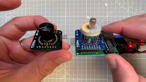
If there’s one thing we like around here more than seeing an improved version of a project we’ve already covered, it’s when the improvements make the original project cheaper. In the case of this LED ring light for pots and encoders, not only is it cheaper than its predecessors, it’s better looking and easier to integrate into your projects.

Right from its start, [upir]’s “Pimp My Pot” project has been all about bringing some zazzle to rotary controls. Knobs with a pointer and a scale on the panel are okay — especially when they go to eleven — but more lights mean more fun. The fun comes at a price, though; the previous version of “PMP” used an off-the-shelf LED ring light with a unit cost of about $10. Not the end of the world, perhaps, but prohibitive, and besides, where’s the fun in just buying a component specifically made for rotary control indication?

The new version shown in the video below is pin-compatible with the driver board [upir] used for the previous version, which is based on the MAX7219 display driver. Modifying the previous board to accommodate 32 white 0402 LEDs over a 270° arc was no mean feat. [upir] covers both creating the schematic and the PCB layout in some detail, providing his usual trove of tool-chain tips for minimizing the amount of manual work needed.

Wisely, [upir] chose to get his boards assembled by the vendor; getting all those LEDs to line up perfectly is a job best left to the robots. While the board is designed for use with pots that mount on either side, we much prefer mounting the pot’s shaft through the board, as it keeps the LEDs closer to the knob. The final price per board works out to about $6.30 in quantities of ten and falls to a trivial $1.70 each for lots of 1,000. Pretty sweet savings on a pretty sweet-looking build.

This is a cool use of a ring of LEDs, but if you prefer the finger kind, you can make that, too. You can do it the easy way or the hard way.

Continue reading “Pimp My Pot Redux, Now Cheaper And Even Better”

NVIDIA Trains Custom AI To Assist Chip Designers

AI is big news lately, but as with all new technology moves, it’s important to pierce through the hype. Recent news about NVIDIA creating a custom large language model (LLM) called ChipNeMo to assist in chip design is tailor-made for breathless hyperbole, so it’s refreshing to read exactly how such a thing is genuinely useful.

ChipNeMo is trained on the highly specific domain of semiconductor design via internal code repositories, documentation, and more. The result is a vast 43-billion parameter LLM running on a single A100 GPU that actually plays no direct role in designing chips, but focuses instead on making designers’ jobs easier.

For example, it turns out that senior designers spend a lot of time answering questions from junior designers. If a junior designer can ask ChipNeMo a question like “what does signal x from memory unit y do?” and that saves a senior designer’s time, then NVIDIA says the tool is already worth it. In addition, it turns out another big time sink for designers is dealing with bugs. Bugs are extensively documented in a variety of ways, and designers spend a lot of time reading documentation just to grasp the basics of a particular bug. Acting as a smart interface to such narrowly-focused repositories is something a tool like ChipNeMo excels at, because it can provide not just summaries but also concrete references and sources. Saving developer time in this way is a clear and easy win.

It’s an internal tool and part research project, but it’s easy to see the benefits ChipNeMo can bring. Using LLMs trained on internal information for internal use is something organizations have experimented with (for example, Mozilla did so, while explaining how to do it for yourself) but it’s interesting to see a clear roadmap to assisting developers in concrete ways.

EcoEDA Integrates Your Junk Bin Into Your Designs

If you’re like us, there’s a creeping feeling that comes over you when you’re placing an order for parts for your latest project: Don’t I already have most of this stuff? With the well-stocked junk bins most of us sport and the stacks of defunct electronics that are almost always within arm’s length, chances are pretty good you do. And yet, we always seem to just click the button and place a new order anyway; it’s just easier.

But what if mining the treasure in your junk bin was easier? If you knew right at design time that you had something in your stash you could slot into your build, that would be something, right? That’s the idea behind ecoEDA, a Python-based KiCAD plugin by [Jasmine Lu], [Beza Desta], and [Joyce Passananti]. The tool integrates right into the schematic editor of KiCAD and makes suggestions for substitutions as you work. The substitutions are based on a custom library of components you have on hand, either from salvaged gear or from previous projects. The plug-in can make pin-for-pin substitutions, suggest replacements with similar specs but different pinouts, or even build up the equivalent of an integrated circuit from available discrete components. The video below gives an overview of the tool and how it integrates into the design workflow; there’s also a paper (PDF) with much more detail.

This seems like an absolutely fantastic idea. Granted, developing the library of parts inside all the stuff in a typical junk bin is likely the biggest barrier to entry for something like this, and may be too daunting for some of us. But there’s gold in all that junk, both literally and figuratively, and putting it to use instead of dumping it in a landfill just makes good financial and environmental sense. We’re already awash in e-waste, and anything we can do to make that even just a little bit better is probably worth a little extra effort. Continue reading “EcoEDA Integrates Your Junk Bin Into Your Designs”

Review: LibrePCB Hits Version 1.0

Nearly three years ago at the start of 2020 and before the pandemic hit, we took a look at an up-and-coming player in the world of PCB design. LibrePCB is by no means as old as the more established players, but at the time it was joining the ranks of open-source EDA packages with its first early stable releases. It showed a lot of promise but was still a little rough around the edges back then, but in the years since it’s advanced to the extent that in September they released version 1.0. That’s a significant moment for any open source package, so it’s time to return and take another look. It’s a cross-platform package with builds available for Linux, Windows, MacOS and FreeBSD, of which I needed the Linux version. There are one or two options to choose from, I went for the appImage as probably the least trouble. Very quickly I was in a new EDA package, and I set out to make a simple Schmitt trigger oscillator as a test project. Continue reading “Review: LibrePCB Hits Version 1.0”