For anyone out there who has ever struggled finding a part for Eagle or KiCad, there are some who would say you’re doing it wrong. You’re supposed to make your own parts if you can’t find them in the libraries you already have. This is really the only way; PCB design tools are tools, and so the story goes you’ll never be a master unless you can make your own parts.
That said, making schematic parts and footprints is a pain, and if there’s a tool to automate the process, we’d be happy to use it. That’s exactly what uConfig does. It automatically extracts pinout information from a PDF datasheet and turns it into a schematic symbol.
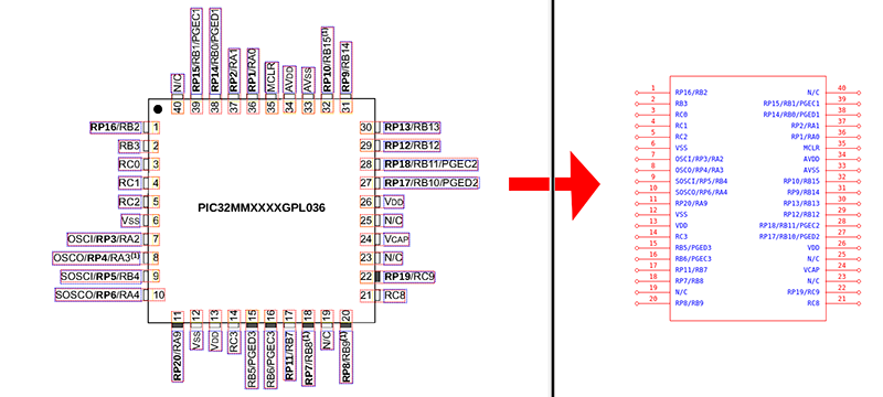
uConfig is an old project from [sebastien caux] that’s been resurrected and turned into an Open Source tool. It works by extracting blocks of text from a PDF, sorts out pin numbers and pin labels, and associates those by the relevant name to make pins. It’s available as a pre-built project (for Windows, even!), and works kind of like magic.
The video demo below shows uConfig importing a PDF datasheet — in this case a PIC32 — automatically extracting the packages from the datasheet, and turning that into a schematic symbol. It even looks as if it’ll work, too. Of course, this is just the schematic symbol, not the full part including a footprint, but when it comes to footprints we’re probably dealing with standard packages anyway. If you’re looking to build a software tool that takes a datasheet and spits out a complete part, footprint and all, this is the place to start.


Hum, this was already posted a month back — https://hackaday.com/2018/09/11/automagic-tool-makes-kicad-schematic-symbols-from-pdfs/
What do you think is worse. Reading about this twice or finding out that a fellow HoD staff wrote about this already?
I wouldn’t know, I don’t know how sensitive the HaD-stuff is on such things. If I really had to hazard a guess, I would imagine them going “Oh well, it happens.” As for reading about this twice, do note that I wasn’t complaining, I just made a mention of it.
Well I for one like seeing Kicad stuff even if it’s just confusing repeats. Beats badges and raspi cases anyday.
Badges and raspi cases designed in kicad are still ok.
It’s all been a bit deja-vuey lately, swear the sodium dumping had an article before, and I first thought the rotten C64 was a repeat, but I think it was a different rotten C64
Probably not enough ???? and I post this at 2:31 am EST????
“That said, making schematic parts and footprints is a pain, and if there’s a tool to automate the process, we’d be happy to use it. ”
Sort of an ABBYY of the electronics world, eh?
Didnt have to read the article. It was already posted before. Great job camping Benchoff
Not his fault necessarily. I’d imagine contributors contribute. Someone ‘at the top’ then chooses the contributions to run. If they’re not at the tech level of the contributors, mistakes will happen.
Hackaday search for interesting items and write articles to present to us, this saves time when not looking for something specific, and can plant seeds for idea’s or solutions.
Its no big deal if something gets repeated, but I really would like a different format for the project pages.
Now do it for PCB footprints…
I have for a long time wondered, why doesn’t kicad have a long thick list of all common packages?
It has most packages, but not really all of them, not to mention that there are duplicates… (An 0805 resistor has the same footprint as an 0805 capacitor or inductor, yet each has their own footprint… Why couldn’t all two leaded devices of that type, 0805, 0806, 0502 etc just be on a list of two pin SMD components?)
Then there is the other standard packages, like dip, sip, sot, etc…
If one told someone that “I have a 44 pin SO package that has a 0.6 mm pin pitch and is 8 mm wide.” Then most people can probably draw that footprint with ease. Yes, this description might not be enough in and off itself, due to various reasons, like is it an 8 mm wide package, or is it between pads, and is that inside or outside width? and so on… And then we could also add the statement “and I want to wave solder it.” and our foot print designer instantly knows we might want solder thieving pads too.
Similar story for many other common packages too. All of them can rather easily just be generated on demand from a short description. And if pins are physically missing on the package, then we could add that to the description. So that practically any package basing on standard footprints would be supported out of the box. Doesn’t matter if it is an 8 million pin staggered into 32 rows on each side of a dip package, having an abysmal 0.2 mm pitch. Our generator would just spit out the result for us to fill out pin names on. (Pin names could likely just be imported from a list, since pin 1 is pin 1 and 2 is 2 and so forth down the list. (and yes, that silly dip package would be 25 meters long…))
And we have the making of schematics symbols, and that is most of the time boxes with pins anyway, so why can’t I just ask for a box with X many pins on y sides, then give names to those pins. While currently sitting and making each pin and not to mention the box manually takes so much time. (Though, if I were payed by the hour and didn’t have a deadline to meet, then I wouldn’t complain about the current implementation…)
All that is really needed though is some industry standard way of describing a footprint, then manufacturers could just add that code to their data sheets and one could just copy and past it into what ever layout tool one has and have the package at hand without needing to draw a single line.
You might want to take a look at https://github.com/pointhi/kicad-footprint-generator and http://kicad.rohrbacher.net/quickmod.php.
I were honestly talking idealistically. I have seen those links before. They are of help, but still not what I outlined.
The idea I stated were simple:
1. The industry needs a standard way of defining any footprint, in text as a “short” code. (So that it is as easy as possible to copy.)
2. All major manufacturers should then preferably use that standard in their data sheets. (and hopefully small manufactures too)
3. You as a designer can then simple copy that code from the datasheet and import it into whatever PCB design tool you prefer using. (Or at least the major ones like KiCad, Altium, Eagle, etc)
4. The program then gives you the footprint to the manufacture’s specifications. (All you did were copy and past and click ok, and there it is! Could it be simpler?)
Things of note though is that the datasheet would likely also contain a code for wave soldering, and one for reflowing, another for hand soldering and so forth. Not to mention codes for each package type that the manufacturer deliver. Though, it is in the end mostly up for the manufacturer to decide what they wish to provide. (But hopefully they give one code for each package at least.)
But in the end, it would save you as a designer all trouble of worrying, since all you need to do is copy the code from the datasheet (where the manufacturer is responsible for making sure that the code is correct.)
And the design tool you import the code into is the developer of that design tools responsibility of making sure that it imports the codes correctly. (Yet again meaning that you have less hassle to deal with.)
But the major thing is that it saves you a lot of time, since there is no need to search through footprint libraries or draw the footprint manually or consort to a wizard that has more options then you care to poke a stick at.
I am though not saying that Wizards and component libraries are bad, as well as drawing footprints manually is all crucial features for those times the manufacturer didn’t give a code for the footprint you need. (Though, you could also just copy the code for the same type of package, but yes, here you are responsible for making sure it is correct.)
But what I am saying is, copy and pasting a simple code is a lot faster and has a lot less hassle. And in the end of the day going to cut down your turn around time for your projects and let you live up to your deadlines with more ease.
Since we have probably all been there at some point, soldering a board for the first time, only to see that one component has the wrong pin pitch…. (Picking the wrong part in the library, or drawing it incorrectly, or feeding the wrong number to the wizard can all happen and yes, we could also just have imported the wrong code. All of those mistakes would likely pass your Design Rule Checking…)
The real solution isn’t a huge list of packages, but a standard compliant footprint wizard.
the IPC-standard allows each manufacturer to have their own tolerances and measurements to common package types such that you’d have to have 0402 package for each manufacturer, and for each of their different products anyway.
Often they do not differ from the median hugely, so that you really can use one package with several manufacturers and products, but it’s more wise to have that 0402 package drawn with the exact specifications from the manufacturer so you minimize the issues with re-flowing.
For example, I’ve had situations where inside the same manufacturers one single family of ceramic capacitors, you have three different physical sizes for “0805”… for example the tolerance can be larger so you need bigger pads for this capacitance/voltage capacitor than this other one or anything like that.
It’s of course understandable that this is to make manufacturing yield larger since troubles usually come about during re-flowing and in large scale manufacturing, but to say that “0805 is 0805” is misleading to say the least, not to mention QFN’s or all other weird and wonderful packages.
Easy and fast to use IPC-compliant footprint wizard.. that’s what kicad really needs to solve this issue. No professional designer wants to draw that package by hand unless they absolutely can’t get it out of the wizard. :)
And to add… we have third party footprint tools for this exact reason. They try to be CAD package agnostic and they follow the standards and all that stuff. But they’re expensive for a reason.
Some good packages like Altium have IPC-compliant wizards, but they have some foolish limitations even though they can do it 95% of the time without issues.
One of the more high end third party IPC-compliant footprint packages:
https://www.pcblibraries.com/Products/FPX/Altium.asp
I repeat: This is not a deja-vu! I repeat: This is not….
Guess Mr. Benchoff needs some cash, and this is just an easy way to get some articles submitted quickly.
:-D
Honestly, I don’t think this is a real solution unless you’re ready to make absolutely sure the tool worked well and there are no errors. After which you might as well do the symbol manually.
The main issue is, that when you copy stuff from a PDF, it can be formatted absolutely weirdly and what you get when you copy an array or a vector picture with text is anyone’s guess. The delimiters are often all over the place and can differ between PDF’s and within a PDF so… it can take a lot of time to get that right. some times I have to use different PDF reader to get the data out of it in any decent shape that doesn’t equate to manually writing everything to get it right.
I do my symbols on spreadsheet first that has columns for different pieces of information about the component pin and rows for pins. After it’s filled by hand and partly by copy pasting the stuff from datasheet (often copying stuff through NotePad++ to make sure it’s formatted correctly and there’s nothing weird), it’s relatively easy to glance over it and make sure there are no mistakes.
After that Altium designer has a tool to import that spreadsheet to a symbol and that’s 95% of a component done… unless the component has weird package then one can’t use the IPC-standard package wizards and it takes a bit more time.
But getting that spreadsheet 100% right is really 95% of the battle and if there’s a mistake there, it will propagate through to the layout and you’ll have to re-spin the board for sure.
So I’d put extra amount of effort and wouldn’t trust a tool to just copy it from the PDF.
You are right, it is difficult to trust a tool like that but you can saw in less that one minute if it fail or not with the pdf debugger view. In case it work, it save you a lot of time, otherwise, do it like you do it normally.
But PDF extraction is not the only functionality of my tool: pinruler is for me more interesting and 100% safe. It permit a reorganization following a set of rules named KSS (Kicad Style Sheet) to place pin with your preferences in seconds. And this step takes a lot of time to do by hands!
So what I have to say is, try it, it 100% free and open. And give your feed back at https://github.com/Robotips/uConfig/issues you will help a lot of hardware dev like us. Thanks!
You don’t trust it… You use it as a starting point.