Even though you can easily order a PCB from any one of a dozen board houses and have it on your desk in a few weeks, there’s still a need for home-made circuit boards. If it’s because you have very special or strange requirements, you want to save money, or you need to suffer for your art, you can make printed circuit boards at home. You can even apply soldermask. It’s easy, and [Renzo] is here to show you how.
The beginnings of this tutorial cover well-tread territory such as building a CNC router, laying out a circuit, and cutting a piece of single-sided, copper clad board. If you stopped right there, after milling traces into a board, you would have a functioning circuit. But it wouldn’t look good; a piece of copper does not a PCB make, and you need soldermask. That’s where the real work comes in.
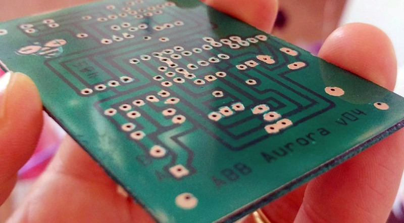
Applying the soldermask meant there needed to be places without soldermask, mostly the vias and through-holes. For this, [Renzo] pulled the copper pad layer out of Fritzing, printed it on a transparency sheet, and finally applied the UV-curing soldermask. This came as a kit, and right now, you can get 10 ml of green, red, blue, yellow, and black UV-curing soldermask, and a UV flashlight for ten dollars on the usual Internet shops. This soldermask was lathered on, rolled out, and exposed with the UV flashlight. After a quick wash in acetone, the result is a perfect PCB.


The original article is cool and well documented but I was this close of not reading it because of “fritzing” in the title, lol!
Damn Benchoff and his anti-clickbait rabble rabble
Not a 500 ball BGA though…
Suggestion for title v2:
“Create LED-Green Colored Soldermasked PCBs for your Arduino, with Fritzing running on a Raspberry Pi 3”
In a *fully 3d printed* case!
not first …
https://www.youtube.com/watch?v=y-bjbF8USHc
Curious why fritzing is important here. Can’t you use any PCB CAD package to print the mask pattern?
Fritzing is actually very good at one thing. It’s great for making graphics.
Every O’Reilly book that deals with electronics, every book that has ‘raspberry Pi’ or ‘arduino’ in the title uses Fritzing for the circuit graphics. Fritzing is really good a placing vector art and drawing wires between pins. It’s great for making pictures of circuits.
Of course, fritzing thinks the connections between parts are ‘wires’ and not ‘nets’, so it completely fails at any real circuit creation, but it’s good at illustrating circuits.
This does not look half bad:
https://hackster.imgix.net/uploads/attachments/619402/wiring-gitlab_fyswcWOqUL.JPG
https://www.hackster.io/arduinoenigma/a-simple-five-button-polyphonic-arduino-uno-based-piano-b367be
Make your way backwards through the Hackaday blog, reading all Brian Benchoff posts, until you achieve enlightenment.
I started with Fritzing but as it hasn’t gotten an update in five years, has no ability to keep your traces aligned with nice curves, following a nice route plus many many other functionality limitations I switched to KiCad. I was up and running in about an hour after watching the digi-key tutorial videos by Shawn Hymel. Sorry but Fritzing is dead end software.
Fritzing is yet another shortcut app for people who don’t want to learn basic, necessary skills like circuit design, simulation, schematic capture, etc., let alone pcb layout. Fritzing and other “lazy person’s shortcut to feeling like an engineer” applications are creating handicaps and teaching bad practices and bad habits while doubly hurting potentially good designers by eliminating the very necessary steps of learning the fundamentals and understanding basic theory and best practices.
I could barely get through this article after seeing Fritzing in the title. It never fails that a young person and/or student comes to an educational forum and asks questions about things they’d be able to easily figure out themselves had they not been handicapped by or developed bad habits from things like Fritzing.