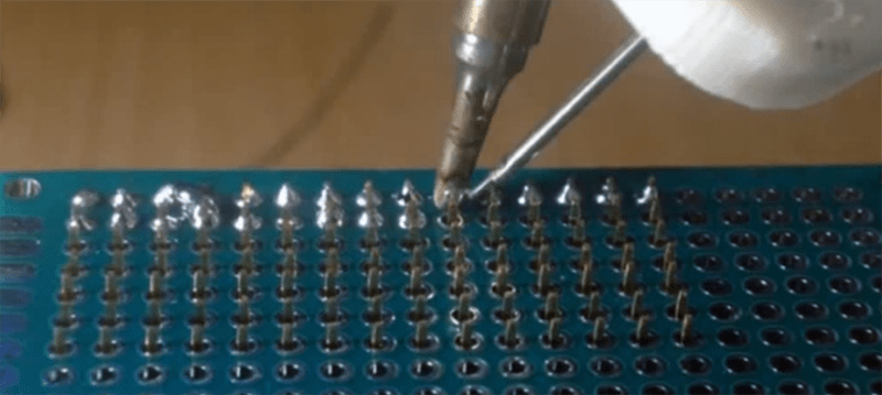
What do you do if you have to solder thousands of through-hole parts? The expensive, professional way of doing this is running the boards through a wave soldering machine, or a machine with a fancy CNC solder fountain. The amateur way of soldering thousands of through-hole joints is putting some boards on the workbench and sitting down with a soldering iron. There is nothing in between; you’re either going to go with full automation for a large soldering job, or you’re doing it completely manually. That’s the problem this soldering robot solves. It’s a small, cheap, but still relatively capable soldering robot built out of a 3D printer.
This project is a solution to the development hell of the OpenScan project. This project is built around a small, simple printed circuit board that uses several 0.1″ female headers to connect an Arduino and motor drivers. Soldering them by hand is simply boring, and 3D printers are cheap, so the great mind behind this project decided to use a printer to pump out solder.
The modifications to the printer include a mount for a TS100 soldering iron and a modified filament extruder that pushes a spool of solder through a PTFE tube. The GCode for this soldering job was created manually, but you could also use a slicer instead. After 20 hours of development, the ‘success rate’ – however that is defined – is between 60-80%. That needs to get up to four or five nines before this DIY soldering robot is practical but this is a decidedly not-bad result for a few hours of tinkering.
This printer mod works great for the use case of stuffing a few 0.1″ headers into a board and letting a robot automatically solder the joints, but this printer will run into a problem with the general case of soldering a lot of randomly-shaped through hole parts. You need to actually hold the parts up against the board while soldering. There’s an easy solution to this problem: just flip the 3D printer upside down. This hack of a cheap 3D printer is so, so close to being a great solution to soldering thousands of through-hole parts quickly and easily, and we’re looking forward to seeing where the community takes this idea. You can check out the video demo below.


Impressive!
Thanks :) And there will be some updates as soon as possible
Thomas, this is a great project. I’m following your steps and building my own. Slightly different choices here and there, but the same principles.
Just wanted to let you know, that your work is an inspiration.
Thanks!! I just checked out the project on your blog and in many ways it looks way more sofisticated! This is just amazing and I will follow the project for further updates.
So, are there any updates?
I suspect that further toolpath tinkering will improve it to a point, but the improvements will plateau soon. The other room for improvement includes:
* Automatic tip cleaning — mount a brass-turnings cleaner to the bed somewhere and visit it periodically?
* Controlling the solder’s position within the needle — some small bends to the needle might make this more deterministic.
* Feeding the solder more slowly, or moving the head slightly during the beginning of feed. When hand soldering, I often feel like the solder’s “just not doing anything” until I wiggle it a bit. I guess this is a toolpath tinker after all.
* Much better workholding for the board! It looks like it moves a lot during the videos. Heck, you could even 3d print a mount with pegs that fit into the mounting holes :)
* A way to cock the component leads to one side of the hole. Respinning the board with staggered holes like https://www.sparkfun.com/tutorials/114 might actually help.
Overall this is a super cool project and I’m likewise excited to see where it goes!
Why isn’t tolerance mentioned anywhere in that sparkfun article? If you stagger the holes, you eat the hole tolerance, both position and diameter
Thank you for your ideas. I’ve already implemented some of your ideas, but did not have the time to make an updated video. First, I’ve modified the toolpath to incorporate a little bit of wiggle, when touching the pin. Furthermore the solder is extruded in two steps, first a little bit, wait 500ms for distribution and then add the main blob + wiggle. Concerning the workholder, yes, this is, what we would call “russian”, but I’ve found out that adding a flexible foam underneath the work helps a lot. This way the soldering iron really pinches the hole and thus makes good contact. Anyway, there are many things to improve, especially the printer’s frame is a big issue…
At the current state, I constantly achieve an accuracy of above 98% (with those implemented improvements) and thus do not feel the need to do any tinkering, as this machine is used as a tool. Anyway, due to the great feedback, I will further push its developement as soon as possible.
This is actually really cool. 80% yield is not great, but I think the usable range starts around only 2 9s I mean 99%. I do that medium volume like hundreds of boards in a sitting and single thousands per year. 99% is comparable to my reflow yield pre-rework. It’s ok to have to touch up one out of a hundred by hand. You made it yourself and you’re good at fixing it. You get used to doing the same reworks and you get fast at it. Being able to rework your own stuff efficiently is one of the strengths you have at the medium volume.
Honestly though in the video the results look really good already, accepting the dismissal of the solder bridges as stated. With only the one example to go on, that looks like a perfectly usable yield. I’m not sure how long it actually took it to solder that, but you know what if I’m not having to do it myself I’m not sure I care.
I like this.
I have to disagree–so what if it’s only doing 80%? He was doing 100% by hand before, now he only has to do 20%.
That’s 80% less solder joints that he has to make, or a 4x increase in production–freeing him up to either solder more boards in parallel or work on other tasks.
Yes, I realize wicking up bridges takes longer than making a joint right the first time, but I have a hard time believing this isn’t a huge net gain in productivity.
Not sure who you meant to disagree with but I quite agree with you. It looks suspiciously usable as-is.
Actually, the video is not up to date and I did not do any updates, as I use this machine as a tool and didn’t think it was worth mentioning (but changed my mind due to the great feedback and overall interest ;). By now I get an accuracy of 98%+ maybe even above 99%. My standard PCB has 64 connectors and usually I have to resolder one of maybe for or five PCBs. Usually the main issue is misplacement of the PCB/touching the weak printer frame and thus deforming it… I will spend some more time on this machine in the future, so i will change it to an Ender3 Frame and maybe turn it upside down, and … There is so much to explore. I just should not forget to do a proper documentation ;)
I was thinking to use a 3d printer to automatize all soldering process of smd components. Including laser soldering.
Why do one solder joint at a time when you can put the whole PCB into a reflow oven?
Because many through-hole components can’t handle being in an oven.
Then you just run it through *then* add the through-hole components.
Only for SMD components, not for through hole
But it would be better to mount everything upside-down, so the components don’t fall…
From a manufacturing point of view, through hole parts are a hassle as they are additional steps required. They use wave soldering for extensive through hole parts and selective wave for boards with partial through hole components. May be intrusive reflow or switch to SMT?
Shitty soldering quality like this would need machine vision for solder joint inspection. Consider a thinner solder, add extra flux, use a different tip and higher temperature setting.
I would love to see a machine doing drag soldering some day.
Or use solder paste instead.
That’s what “Intrusive reflow” means…
http://www.epdtonthenet.net/article.aspx?ArticleID=8507
To be fair, the above shown video is not very actual (as I did not get to updating it). Here you can see a “newer” version with the improved toolpath: https://www.instagram.com/p/BrIBXYnH7yx/
Since then the accuracy is above 98% and the overall quality of the joints greatly improved. Anyway I do test all PCBs manually to ensure quality
Are you telling me someone has added another potential fire risk to the already infamous spontaneously combusting Anet A8. I wonder if fire risks add linearly or exponentially….
Derp.
He’s right you know. I’m in a printer group on Facebook and I frequently see burning issues with anet printers, particularly on their connectors
Sure the Anet A8 is well-known for its fire hazard. There are two things to keep in mind, I do not use the heated bed nor the heating element on the extruder. The soldering iron is directly connected to the PSU and the mainboard is only running the stepper motors. So way less power is needed compared to the 3d printer setup.. Anyway I would never leave my machines unattended ;)
The “easy amateur way” is to mount all the components to the board, apply and solder paste to the leads at the thru holes then hit it with a hot air iron or oven.
Interesting, but I think that would take almost exactly the same amount time per pin. Since you still have to hit every pin with a tool for a second or 2.
Tried that, but melted the plastic on the connectors. By the time the board heated enough for the solder to melt the connector plastic housing was completely destroyed.
You can reflow many through-hole parts by just using a thicker ~0.2mm stencil (you can e.g. 3D print it) and hot air. It depends on ratio of pad size vs. hole size.
If all parts are the same height, you can support them easily enough on table. If they are different heights, you can use high-temperature glue like used for double-sided SMD reflow. Or you can make a jig from high-temperature silicone with holes where you can put the parts before putting the PCB on top.
> That needs to get up to four or five nines before this DIY soldering robot is practical
Why? Can’t you just test the boards?
When I saw the headlines I thought “why” and “what a nonsense, this would never work blablabla…” then I started reading and I came to my senses… and I realized that this is actually quite a fun project with lot’s of interesting challenges.
Yet I have my doubts about the labor time that is being saved here… the time investment in the device itself… then when it finally works then checking all work it’s done, also baby sitting while it operates etc. But other then that, the project is really fascinating and when it works properly it will be so satisfying to watch. So good luck with this project and I hope it all works out.
You really don’t have to baby sit a properly dialed in and setup 3d printer, I don’t see why the same would occur here.
You do have to baby sit it during calibration and testing, which is what OP is doing since this is an entirely new design
Actually this machine has already saved me 20-30h (even including its developement, which was fairly straight-up). Usually I run this machine next to my workbench, where I do manual soldering + placing components on the machine every 5-10 minutes+dialing it in. One PCB with 64 joints takes less then a minute in placing the parts+starting the soldering process. And I would never be able to do those number of joints in a minute… Concerning testing, as these PCBs are handsoldered, I perform functional tests anyway, so the use of this machine does not add any time to this…
Gcode from solder mask is what is needed.
A friend wrote me a small GUI on a script, that creates the Gcode for this machine from a Gerber file’s drill pattern. I can hopefully publish the program as soon as I get his agreement
Soldering robots have been (ree-) invented many times, and are even commercially available. Many youtube video’s, some lead to projects with documentation.
I’ve done a lot of research on this topic, and yes, those machines are readily available but usually have a massive price tag. If I am wrong or just did not find the right project, I would be very happy if you could add a link or any ressources for sub 100€ soldering machines ;)
This printer mod works great for the use case of stuffing a few 0.1″ headers into a board and letting a robot automatically solder the joints.
http://thebest3dprinters.com/
looks good. However, for good solder connections after applying solder I usually let it ‘bubble’ for a second or two, whilst still touching the solder iron tip to the connection. That’s how I’ve been taught to do it, supposedly to give the flux a chance go make a good connection.
Actually this is usually how I do it by hand:
1) apply soldering iron to both metal bits that need soldering, so they warm up.
2) apply a tiny bit of solder to make a good heat conduction to the metal parts and to allow some flux to do its work
3) apply the main blob of solder that forms the connection
4) let it bubble for a second or two
I was also taught to “bubble”.
During my training it was heavily impressed on me to do:
1) apply soldering iron to the pad on the PCB, not touching the pin of the component for 1s
1.5) move the iron to the pin so both the component pin and PCB pad are heated
…
The bubbling is no goal in itself, but the flux needs time to do its work, and sometimes you can clearly see that the wetted part slowly increases after the solder is applied.
The amount of bubbling also varies widely. The blue experimental PCB’s I bought from Seeeeed outgassed the most. So much even that it becomes annoying (Sometimes it’s violent enought to splatter the solder away). Single sided PCB’s do not bubble at all. Any outgassing simply vents to the other side of the PCB.
Also, when you have a decent stereo microscope you do not have to abide by those rules of thumb and you actually see what is happening. If you want to buy a stero microscope, a zoom range between 5x and 15x is about ideal. Some of the cheaper stereo microscopes have fixed magnifications of 20x and 40x and these amplify too much for soldering, and are not fit for electronics work.
Thanks for your detailed description, actually I’ve implemented this routine almost identically in the gcode. By this improvement the overall reliability increased drastically. I hope to get a better documentation on this project very soon, where I will describe the toolpath for each joint in detail.
Hi Thomas, did you end up doing the documentation? Very interested in doing my own machine
you can buy one from robotdigg, https://youtu.be/lmdXfnTqBu0
Super cool project and a very clever re-purposing of 3D printing technology!
You realize that when younget this dialed in the next step is a 3d converted into a pick n place machine! With those two going you could really blast thru a bunch of boards. I do one thing by hand in batchs of 500 because itsba sensor board and most componets i used are thru hole. This is a fantastic exciting project please keep on it!