Digital design is hard. But in the right environment, digital circuits are more forgiving than analog. That 3.3V signal coming out of the chip has to drop a lot along the way to not be a logic level at the destination. If you are trying to push the boundary then digital design has much of analog design, but mostly you get a bit of a pass on many things that plague analog designers. Berkeley’s AI research group has been experimenting with using deep learning to evolve analog IC design.
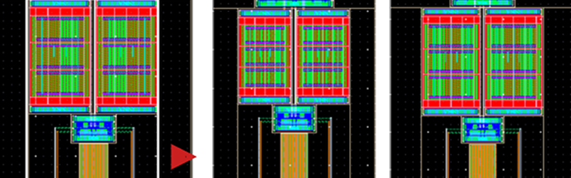
Analog ICs are plagued with noise sources and often don’t have the margins that digital circuit designers enjoy. According to the post by [Kourosh Hakhamaneshi], designers often build a few blocks and attempt to lay them out in a way that should work and meet other requirements. Then they employ simulation, make changes as required, and simulate again. Accurate simulations can be very time intensive. You can read the actual paper, too, should you want to dig into the details.
The problem is really one of optimization. An amplifier for example might need a minimum gain and bandwidth. In addition, there is always the need to take up as little space on the die as possible — just as you don’t want to waste space on a PCB. Since simulation is so expensive, the work appears to try to train a neural network to determine if one design is better than another based on the desired design criteria.
The result isn’t quantitative, but knowing which of two designs is better is very useful for selecting candidates to test in simulation. Interestingly, according to the post, it sounds as if the learning model trains itself on random permutations of the exact circuit you want to design — which makes sense. This training corpus requires simulation, of course, so that eats into the potential savings.
This technique could have applications with other optimization problems, too. We generally like simulation, even if ours don’t usually take that long. Our favorite one is pretty simple and runs in a browser.


This reminded me of a little distributed computing project (BOINC style) many years ago, which used genetic algorithms (?) to design fault tolerant digital circuits… does anyone know the name of this project? I can’t remember it and couldn’t find anything doing a search using the vague details I can remember =/
Simulating analog behavior in a chip can indeed be a complex and time consuming en devour. That sometimes needs a supercomputer to be done in a timely fashion.
So proper circuit simulation can be very processor heavy, there is other methods to “solve” this problem.
One simple solution is to never simulate the whole chip at once, and only do parts of it. Downside with this is that the chip might not “work”, since major parts of it aren’t there.
Another solution is to make the simulation simpler, though with the downside of usually being less accurate, but this might not matter much during development. (one should still likely do the occasional validation of the circuit (full on simulation of the whole thing), to see that it actually is moving in the right direction.)
Here we would first break down the whole chip into parts, then characterize those parts, as to make a more simplified model of the chip.
A very simple example would be simulating a wire by the use of a FIFO buffer. After all, we know its length and thereby its delay. (Though, this approach would not account for cross talk, mismatched terminations/impedance etc… Though, each of these things can also be characterized. And worst case, one needs to break up model of the wire into a few more segments.)
One can also characterize amplifiers, filters, etc. After all, characterization would technically be simulation in and off itself, but only of one smaller part of the system as to get a model of its behavior over a wide range of inputs etc, and if you have many “identical” parts of the thing you desire to characterize, then you don’t need to simulate it for the other parts. (since they are “identical”, then you have just simulated and characterized all of them.)
Since the “identical” parts statement is also still true if you move the thing to a different place on the chip, or duplicate it, etc. As long as one doesn’t change the physical design of the part, the characterized model of it will remain true.
Characterization will allow one to not really need to simulate a lot of things. For example, simulating a multi stage filter is not all that fun, while a characterized model of its behavior could be fairly trivial to deal with. (and yes, how it effects ground/power and other signals in its vicinity needs to be part of that model. But hopefully it is well isolated from random signals, otherwise that can destroy the validity of the “identical” statement above.)
Downside, the characterization of the parts is a more simplified model compared to a proper simulation, and might not reflect reality as accurately as needed for final circuit validation. But, it can still speed up development.
The accuracy of the characterization is obviously greatly impacted by how well one has characterized the part, and what one has characterized about it. For an example, knowing how a filter effects the ground conductor is important, since it can in turn effect other signals/components.
In the end, this wouldn’t really replace simulating the whole chip at one point or another, but rather speed up the quick prototyping of the circuit.
Using an AI/NN for chip design seems like just another improper use of neural networks just because “every man and his dog does it, so why can’t we?”
The problem with chip design usually isn’t making fairly arbitrary design iterations. (the main way to train NNs)
But rather to simulate those design iterations. (Something that can cost thousands of dollars in just electricity, for more complex chips.) So how many iterations does it take to train a neural network?
Though, one can start training with a tiny circuit, and then go towards bigger things over time, but it is still quite the investment, and how big of a computer will it in turn need to do a “good” job?
@Alexander Wikström,
I agree, if you hand microelectronic analog circuit simulation to AI, you’ll die of old age before it finishes. They should fix quantum computing FIRST, then give then sim to the AI.
[Comment Post Attempt #1]
WOW! The reply comment actually posted the first time -AND- it posted in the correct location!
[Comment Post Attempt #1]
What is more costly, simulating the circuit or physically building it and testing it? If simulating is that intensive and if it was possible to automate the building and testing of select random permutations, then maybe that could be used as a tool to map out the domain of good designs. Just a thought.
The problem with “rapid prototyping” in the semiconductor industry is that it first of takes many days, and secondly is expensive as hell. But yes, it is still a thing that at times gets done. For various reasons, like software simulations might need far more time consuming even on a super computer then just building the thing.
If one goes the maskless or masked route is though a different question. The advantage with photomasks is generally that one can make many chips and do fast exposures, while maskless has the advantage of being able to do anything (within its resolution) but tends to need hours for each exposure. (So if one works with something that only has X amount of working time, then maskless might be out of the picture already.)
Rapid prototyping can though be fairly quick if one doesn’t want to do too many or large things. Even when it comes to maskless lithography. (unless one does high res raster scanning… But the industry is moving towards vector scanning.)
Though, for a lot of digital chips, one practically might not even need to simulate it a lot of times. Because it can be so simple and one has the experience so that it should just work. (Though, always fun to design a chip only to have the power plane blow…)