Computers can write poetry, even if they can’t necessarily write good poetry. The same can be said of routing PC boards. Computers can do it, but can they do it well? Of course, there are multiple tools each with pluses and minuses. However, a slick web page recently announced deeppcb.ai — a cloud-based AI router — and although details are sparse, there are a few interesting things about the product.
First, it supports KiCAD. You provide a DSN file, and within 24 hours you get a routed SES file. Maybe. You get three or four free boards –apparently each week — after which there is some undisclosed fee. Should you just want to try it out, create an account (which is quick and free — just verify your e-mail and create a password). Then in the “Your Boards” section there are a few examples already worked out.
We haven’t tried the service yet, but reading notes from people who have doesn’t give us a great feeling. Apparently, the router only wants two-layer boards with a limited number of wires, for the free version at least. One user reported they used up all three boards and only got error results back.
The real question is do we need AI routing? If you have parts well placed, routing isn’t that hard and there are other autorouters that can do a great job. Of course, many people won’t want to trust their designs to a cloud service. However, the technology could be interesting, especially if it could move things around and work towards different goals (e.g., low noise, minimum size, etc.).
There are others, of course. Then again, you can do it all on the cloud, if you like.
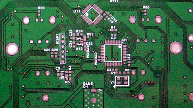
We couldn’t see a picture of an example PCB from the system, so our header image comes from a different source. c-g. [CC BY 2.0]


> You provide a DSN file, and within 24 hours you get a routed SES file
Don’t know about anybody else, but I get a mechanical turk vibe when an automated system takes 24 hours to produce a result.
Setup website, get a bunch of people to sit there taking dsn files, feeding them into FreeRouting, tweaking if easy to finish the routes manually, or send back errors if not.
Hey, it gets better… after a few weeks you see your widgets on Taobao! :-)
That’s what I thought. Each design is probably review by a engineer for it’s sales potential :) Hence the 24 hour delay.
Autorouter does not really need to know what components are on the board. It just connects pads. Maybe you can tell the component package.
Considering how easy it is just to copy a PCB after it is manufactured, why would they go through all this trouble? Just let the designer prove it is marketable before cloning.
Agreed! And PCB alone is far from the end product, it doesnt give you the function, software, packaging, etc.
Yep. Classic ai scam happening here. This can be taken care of just fine with classical algorithms, doesn’t need no buzzwords. They’re just taking advantage of the fact that even obscure, shady projects get a lot of attention if the letters “ai” or “ml” are attached. Bet the non-disclosed fee is steep. I can’t fucking wait for the next ai winter. It’ll do way more good than harm.
I agree that this is a curious use of ai – possibly not at all. However, the buzziest of buzzwords is “ai winter.”
> doesn’t need no buzzwords
So what buzzwords does it need then?
It has to get scanned for IP that may help Uncle Xi first. One has to wonder if there is a dedicated employee at these Chinese fab shops looking for the next big idea that got uploaded.
And all your design are belong to them ? We shouldn’t be mixing cloud and design. Really.
Interesting. I was expecting AI to be available soon in PCB design. The problem arises here it’s a blackbox. For it to be useful we need at least some insight in why the AI routes the way it does. You do need the design files and check it very carefully. For some applications the auto router does a good job and I’m glad it exists.
When designing a PCB there are a lot of little details that need to be just right. Often balancing thermal pad size for dissipation, parasitic capacitance and board volume. Balancing manufacturability versus functionality. How will the PCB be used? Where are the mounting holes and how does the PCB flex? What are the recommendation from the component manufacturer? What are the design guidelines for a similar design? Complex prints I don’t trust to the auto router. Easy projects it will take me a few hours to route it by hand.
We do need more and better tools. Signal return path, EMC, manufacturability, thermal, and Physics of failure. There are tools but they are not that useful and too expensive. Hopefully it will be come standard in the future like protocol analysers on oscilloscopes.
To make this work, AI can only make suggestions but still have to follow routing constrains and design rules. AI cannot change the rules of physics and have to follow it. For very large designs, autorouters with tons of SI based constraints was the only way to get it done. After that, the layout people can tweak the layout.
How large was it? Let’s say our CAD vendor (one of he big ECAD players) had to recompile their suite to handle our large design.
> Where are the mounting holes and how does the PCB flex?
We had a conference call with a subcontractor and one of the questions asked was how to deal with large ceramic caps stresses when PCB flexing on a module. My younger self told them to line up the caps to the shorter axis of the rectangular PCB. I had never have to deal with that myself, but that was the sensible solution on the spot. I doubt an AI can think of that at least in the near future.
check out https://theopenroadproject.org/ this is DRDO supported program they are building open source tool that will automate RTL to GDS flow completely it will generate board design as well. link for ERI summit talk-> https://www.youtube.com/watch?v=pJubnAN3VKw
I would like to see some routed PCBs. Do they have any example to show us?
It’s always a good idea to read to the end before asking questions.
Except the last statement didn’t answer the above question. It just states HaD couldn’t find an answer.
Then in the “Your Boards” section there are a few examples already worked out.
I wonder how it compares to output of mihosoft freerouting…
its no longer possible to register new accounts
“Due to overwhelming demand, we cannot create an account for you right now.”
It has started designing cleverer ai’s which are now getting even cleverer ai’s routed to make even cleverer ai’s, ysing up all the available accounts. Should have Skynet by Thursday.
Dang. Skip the web server. FreeRoute does the job for me, I just want a better UI or integration with KiCAD
Once someone has proven an feat is possible tnen it’s only a matter of time before the result is replicated.
Would be interesting if it could optimize placement as well. Even better if it could recognize which parts not to move if not specified otherwise like connectors.
So I’m thinking about iterative routing, and imagining spreading fractal trees cascading exponentially into alternatives each of which must be evaluated, and start to think that quantum computers better handle this crap or I’m moving to a more technologically advanced part of the galaxy.
I can’t wait for Quantum (Computer) Winter…
I did cloud PCB design long before it was a thing!
I’d apply power to my design and I’d get a cloud!
Miagic smoke? (snicker…)
“Due to overwhelming demand, we cannot create an account for you right now.”
Really??? Really??? Even if this is an AI, this looks like a sales pitch or a scam…
it certainly is
Hi everyone, Nabil the DeepPCB team lead here, first thank you for the interest and comments we did not expect we would appear in Hackaday so quickly :) We’ve reviewed carefully the different points made. First the good news, we’ve just released more capacity so you can subscribe to the system now! If you register you get 4 free runs per week. If you are curious about how DeepPCB works here are more comments:
“ I would bet they have a human in the loop”: No our system is fully automated (which is why it’s a first) so bear with us as we are in beta :) Automation is possible because we use Reinforcement Learning (RL), an AI technology which is very useful for decision-making problems like PCB Routing. At InstaDeep, we deploy RL systems in the real world and work closely with hardware partners such as Nvidia (we’ve recently been upgraded to preferred partner) and Intel (we’re part of the AI Builder Program). In our opinion, having no-human in the loop is critical to accelerate PCB development cycles, and that’s a key feature of DeepPCB. The reason why we need 24 hours is because of our machine learning system that learns to solve boards progressively. To further highlight it, we are actually going to upgrade DeepPCB to show intermediate boards (as it’s being processed) to showcase how our AI progressively improves the solutions it finds.
To tell you more about our company, InstaDeep has built credibility in AI circles by innovating Machine Learning and Reinforcement Learning (RL) to find good solutions to NP-Hard problems. For example, you can check our R2 paper about AI for Bin Packing which was accepted at the NeurIPS 2018 in the Deep RL workshop. More recently we’ve just published a joint AI-research with Google DeepMind that earned a top 2% global ranking at NeurIPS 2019. We also have specific domain expertise in Hardware: some of our team members (me included) have worked for more than 15 years in this field in companies such as STM, NXP, Dialog, etc. We believe it’s an exciting time to be working on PCB Routing, an NP-Hard problem.
On a final note, keep in mind we’re in early beta and our goal is to hear from you to iterate and improve the product better. Things might break from time to time and we’ll certainly make mistakes but what matters to us to keep working hard and make progress on this exciting problem. We believe it’s the combination of Hardware domain expertise and advanced AI know-how that ultimately will yield strong results. If you agree, don’t hesitate to reach out at support@deeppcb.ai we’d love to hear from you!
deepPCB is trying to sell an AI product with a promotion video (https://www.youtube.com/watch?v=zonBeIe2TVE) which is actually a board that has been designed/routed by hand with a great deal of effort and they don’t even acknowledge or mention the authors. Your “credibility” means nothing to me.
http://www.proyecto-ciaa.com.ar/devwiki/doku.php?id=desarrol…
https://github.com/ciaa/Hardware/tree/master/PCB/ACC/CIAA_AC…
deepPCB is simply a big fraud!
not sure if the links work, here is the wiki of the project again https://bit.ly/36iuV0Y
https://github.com/ciaa/Hardware –CIAA-ACC
Hello Ardi !
This is Nabil, the Hardware team lead at InstaDeep. The promotional video is just that, a 3D illustration of a routed board. We’re not claiming we routed it, it’s just there for illustration purposes. The board has a Modified BSD licence on it, which means we can use it, but we are contacting Proyecto-CIAA in any case. Importantly, our service is live, it’s free and designed to help the open source community. We are a young startup and have worked on DeepPCB for more than a year, it’s a genuine innovation and we recommend you use it to have an informed opinion.
Best,
Nabil
Uh, or you can just spend the money on real PCB cad software (I favor Proteus Design Suite) and their router works “automagically” in seconds pretty dang well – no need to send your IP off into the wilderness…. Is it an investment? Sure… Will you ever make money without spending money? Never…
This tech is already here for routing chip designs better than any human. It will soon be here for kicad too because it all moves insanely fast now. Gpt knows how to write kicad.