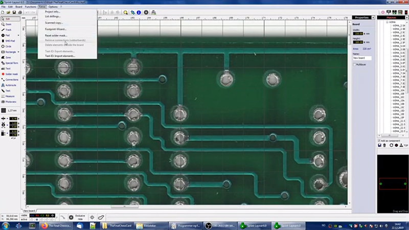
[Bwack] had some scanned pictures of an old Commodore card and wanted to recreate PC boards from it. It’s true that he could have just manually redrawn everything in a CAD package, but that’s tedious. Instead, he used SprintLayout 6.0 which allows you to import pictures and use them as a guide for recreating a PCB layout.
You can see the entire process including straightening the original scans. There are tools that make it very easy to place new structures over the original scanned images.
One might think the process could be more automated, but it looks as though every piece needs to be touched at least once, but it is still easier than just trying to eyeball everything together.
Most of the video is sped up, which makes it look as though he’s really fast. Your speed will be less, but it is still fairly quick to go from a scan to a reasonable layout.
The software is not free, but you can do something somewhat similar in KiCAD. The trick is to get the image scaled perfectly and convert it to a component on a user layer. Then you can add the new component and enable the user layer to see the image as you work. There’s even a repository of old boards recreated in KiCAD.
There are probably an infinite number of ways to attack this. An older version of SprintLayout helped with the Re-Amiga 1200.


For those looking for FOSS options, gEDA PCB has been able to do this since at least 2007, iirc
http://www.delorie.com/pcb/bg-image.html
plus pcb-rnd supports it as well, and can also import eeschema netlists and export Kicad layouts and a few other formats.
I did this as part of one of my projects, and note that large boards will be difficult.
Any angle of the camera relative to the board will cause the rectangular board image to be a trapezoid, and one side will be foreshortened relative to the other side. The effect is small and not a problem with viewing, but when overlaying perfectly straight lines or the corresponding image of the other side of the board things won’t line up properly.
If the board is small, the deviations are also small (less than half a pad width is good) and you can work around the issue. For larger boards, pads start to miss and overlaying the cris-crossing lines on the image becomes difficult to see.
A leveled camera mount and centering the board in the camera view might help.
https://hackaday.io/project/4689-improve-the-haber-process/log/16375-reverse-engineering-a-cheap-ebay-ultrasonic-power-supply
That’s why you need a flatbed scanner for these types of projects.
You can correct for that kind of distortion with a transformation in software. I bet some fiddling with OpenCV could even automate it by finding the outline of the board and transforming it to be square.
Use hugin to correct the perspective. It also allows you to combine multiple images.
You can always scan the board on a flatbed scanner.
Can I use a Laserget Scanner.
There is a project (1801BM1) where the guys used this feature to re-create the layout of some decapped ICs, they did it with the metal and polysilicon layers.
I’ve used this product since 2002 for hobby work. Well worth the price you pay. (For when you just want to make a PC board… not wrack your brain trying to remember how to get EAGLE or whatever EDA tool to just do what you want)
I second this. I too have been using this software for many years. Reasonable price and quick to just bash something out. I’ve used it as above to ‘digitize’ photos of boards. It will also import Gerber files so you can rework them.
Sprint is quite nice for this kind of reverse job. I dd the Amiga 1200 and ever larger the Amiga 3000 for my ReAmiga projects.. have even done some 6 layers cards even if sprint only supports 4 layers.
it requires quite a lot of work as you have no schematictestings etc. but for sure doable..
Chucky, I have been inspired by your ReAmiga projects. I retraced the KU-14194 C64 motherboard in sprint and imported it in KiCad. Made schematics and got the thing design rules checked. I was thinking of doing something like this with your ReAmiga projects. Do you know if there are KiCad schematics out there ? Perhaps Eagle ?
So far what I know there is no such thing. and I have so crazy many projects I cannot find time to do it myself.
I however know of a project to do the Amiga 3000 in eagle. but it will take some time before it is finished.
Are there any semi-automated reverse engineering solutions? It would be nice to not have to to paint over all the traces…
No idea why there are a few very nice Russian origin niche PCB software.
Whats that one that produces curved traces?
Sure beats using a printed scan of the board and crossing off each trace as you map it to the board software.
Now if only there was something that could auto import from scans of schedule layouts, instead of doing similar to the above.
Been there, done that for the TP-Link TL-WR703N pocket Wi-Fi router:
https://github.com/Squonk42/TL-WR703N
From the reconstructed board, you can get the netlist and rebuild the schematics from it.
Huh. Thanks for pointing out the tool and re-created computer boards. I hadn’t run across them previously.
I did this with a 4 layer PCB. I used Office Lens for taking the photos of the top and bottom of the board (correcting for angle), then used a sanding belt to shave off each layer until it was exposed then polishing off by hand to ensure i didnt take away any tracks. Once complete, I used GIMP to scale and resize each photo to exactly the same size, and then used multiple layers and transparency to ensure each via was aligned.
After that, all images were cropped to exact PCB size and exported to individual files for import into Sprint Layout.
In sprint, I would load each layer and trace each component and track on a separate layer including vias.
Then the hard part was to follow each track and then draw it up on EasyEDA for full reverse engineering.
The whole process took about a month, an hour a night – maybe 20 hours or so total?
Well worth it as I know have a full schematic of the board.
As far as I am aware, there is no automated method for tracing tracks.
I believe it works nicely for simple stuff, but once you get into 4-layer and bigger boards, it becomes impossible quite easily. Otherwise nice…